
ESP32-S3 Series
Datasheet
2.4 GHz Wi-Fi + Bluetooth
®
LE SoC
Supporting IEEE 802.11b/g/n (2.4 GHz Wi-Fi) and Bluetooth
®
5 (LE)
Including:
ESP32-S3
ESP32-S3FN8
ESP32-S3R2
ESP32-S3R8
ESP32-S3R8V
ESP32-S3R16V
ESP32-S3FH4R2
Version 1.8
Espressif Systems
Copyright © 2023
www.espressif.com

Product Overview
ESP32-S3 is a low-power MCU-based system on a chip (SoC) with integrated 2.4 GHz Wi-Fi and Bluetooth
®
Low Energy (Bluetooth LE). It consists of high-performance dual-core microprocessor (Xtensa
®
32-bit LX7), a low
power coprocessor, a Wi-Fi baseband, a Bluetooth LE baseband, RF module, and numerous peripherals.
The functional block diagram of the SoC is shown below.
Espressif ESP32-S3 Wi-Fi + Bluetooth
®
Low Energy SoC
Power consumption
Normal
Low power consumption components capable of working in Deep-sleep mode
Wireless Digital Circuits
Wi-Fi MAC
Wi-Fi
Baseband
Bluetooth LE Link Controller
Bluetooth LE Baseband
Security
Flash
Encryption
RSA RNG
Digital
Signature
SHA AES
HMAC
Secure Boot
RTC
RTC
Memory
PMU
ULP Coprocessor
Peripherals
USB Serial/
JTAG
GPIO
UART
TWAI
®
General-
purpose
Timers
I2S
I2C
Pulse
Counter
LED PWM
Camera
Interface
SPI0/1
RMT
SPI2/3
DIG ADC
System
Timer
RTC GPIO
Temperature
Sensor
RTC
Watchdog
Timer
GDMA
LCD
Interface
RTC ADC
SD/MMC
Host
MCPWM
USB OTG
eFuse
Controller
Touch
Sensor
RTC I2C
RF
2.4 GHz Balun +
Switch
2.4 GHz
Receiver
2.4 GHz
Transmitter
RF
Synthesizer
Fast RC
Oscillator
External
Main Clock
Phase Lock
Loop
Super
Watchdog
CPU and Memory
Xtensa
®
Dual-core 32-bit LX7
Microprocessor
JTAG
Cache
ROM
SRAM
Interrupt
Matrix
Permission
Control
World
Controller
Main System
Watchdog
Timers
ESP32-S3 Functional Block Diagram
For more information on power consumption, see Section 3.2.1 Power Management Unit (PMU).
Espressif Systems 2
Submit Documentation Feedback
ESP32-S3 Series Datasheet v1.8

Features
Wi-Fi
• IEEE 802.11b/g/n-compliant
• Supports 20 MHz, 40 MHz bandwidth in 2.4 GHz
band
• 1T1R mode with data rate up to 150 Mbps
• Wi-Fi Multimedia (WMM)
• TX/RX A-MPDU, TX/RX A-MSDU
• Immediate Block ACK
• Fragmentation and defragmentation
• Automatic Beacon monitoring (hardware TSF)
• 4 × virtual Wi-Fi interfaces
• Simultaneous support for Infrastructure BSS in
Station, SoftAP, or Station + SoftAP modes
Note that when ESP32-S3 scans in Station
mode, the SoftAP channel will change along with
the Station channel
• Antenna diversity
• 802.11mc FTM
Bluetooth
• Bluetooth LE: Bluetooth 5, Bluetooth mesh
• High power mode (20 dBm)
• Speed: 125 Kbps, 500 Kbps, 1 Mbps, 2 Mbps
• Advertising extensions
• Multiple advertisement sets
• Channel selection algorithm #2
• Internal co-existence mechanism between Wi-Fi
and Bluetooth to share the same antenna
CPU and Memory
• Xtensa
®
dual-core 32-bit LX7 microprocessor,
up to 240 MHz
• CoreMark
®
score:
– 1 core at 240 MHz: 613.86 CoreMark; 2.56
CoreMark/MHz
– 2 cores at 240 MHz: 1181.60 CoreMark;
4.92 CoreMark/MHz
• 128-bit data bus and SIMD commands
• 384 KB ROM
• 512 KB SRAM
• 16 KB SRAM in RTC
• SPI, Dual SPI, Quad SPI, Octal SPI, QPI and OPI
interfaces that allow connection to multiple flash
and external RAM
• Flash controller with cache is supported
• Flash in-Circuit Programming (ICP) is supported
Advanced Peripheral Interfaces
• 45 × programmable GPIOs
• Digital interfaces:
– 4 × SPI
– 1 × LCD interface (8-bit ~16-bit parallel
RGB, I8080 and MOTO6800), supporting
conversion between RGB565, YUV422,
YUV420 and YUV411
– 1 × DVP 8-bit ~16-bit camera interface
– 3 × UART
– 2 × I2C
– 2 × I2S
– 1 × RMT (TX/RX)
– 1 × pulse counter
– LED PWM controller, up to 8 channels
– 1 × full-speed USB OTG
– 1 × USB Serial/JTAG controller
– 2 × MCPWM
– 1 × SD/MMC host controller with 2 slots
– General DMA controller (GDMA), with 5
transmit channels and 5 receive channels
Espressif Systems 3
Submit Documentation Feedback
ESP32-S3 Series Datasheet v1.8

– 1 × TWAI
®
controller, compatible with ISO
11898-1 (CAN Specification 2.0)
• Analog interfaces:
– 2 × 12-bit SAR ADCs, up to 20 channels
– 1 × temperature sensor
– 14 × touch sensing IOs
• Timers:
– 4 × 54-bit general-purpose timers
– 1 × 52-bit system timer
– 3 × watchdog timers
Low Power Management
• Power Management Unit with five power modes
• Ultra-Low-Power (ULP) coprocessors:
– ULP-RISC-V coprocessor
– ULP-FSM coprocessor
Security
• Secure boot
• Flash encryption
• 4-Kbit OTP, up to 1792 bits for users
• Cryptographic hardware acceleration:
– AES-128/256 (FIPS PUB 197)
– Hash (FIPS PUB 180-4)
– RSA
– Random Number Generator (RNG)
– HMAC
– Digital signature
Applications
With low power consumption, ESP32-S3 is an ideal choice for IoT devices in the following areas:
• Smart Home
• Industrial Automation
• Health Care
• Consumer Electronics
• Smart Agriculture
• POS machines
• Service robot
• Audio Devices
• Generic Low-power IoT Sensor Hubs
• Generic Low-power IoT Data Loggers
• Cameras for Video Streaming
• USB Devices
• Speech Recognition
• Image Recognition
• Wi-Fi + Bluetooth Networking Card
• Touch and Proximity Sensing
Espressif Systems 4
Submit Documentation Feedback
ESP32-S3 Series Datasheet v1.8

Contents
Note:
Check the link or the QR code to make sure that you use the latest version of this document:
https://www.espressif.com/documentation/esp32-s3_datasheet_en.pdf
Contents
Product Overview 2
Features 3
Applications 4
1 ESP32-S3 Series Comparison 10
1.1 Nomenclature 10
1.2 Comparison 10
2 Pins 11
2.1 Pin Layout 11
2.2 Pin Overview 12
2.3 IO Pins 16
2.3.1 IO MUX and GPIO Pin Functions 16
2.3.2 RTC and Analog Pin Functions 19
2.3.3 Restrictions for GPIOs and RTC_GPIOs 20
2.4 Analog Pins 20
2.5 Power Supply 21
2.5.1 Power Pins 21
2.5.2 Power Scheme 21
2.5.3 Chip Power-up and Reset 22
2.6 Strapping Pins 23
2.6.1 Chip Boot Mode Control 24
2.6.2 VDD_SPI Voltage Control 24
2.6.3 ROM Messages Printing Control 25
2.6.4 JTAG Signal Source Control 25
2.7 Pin Mapping Between Chip and Flash/PSRAM 26
3 Functional Description 27
3.1 CPU and Memory 27
3.1.1 CPU 27
3.1.2 Internal Memory 27
3.1.3 External Flash and RAM 27
3.1.4 Address Mapping Structure 28
3.1.5 Cache 29
3.1.6 eFuse Controller 29
3.1.7 Processor Instruction Extensions 29
Espressif Systems 5
Submit Documentation Feedback
ESP32-S3 Series Datasheet v1.8

Contents
3.2 RTC and Low-Power Management 30
3.2.1 Power Management Unit (PMU) 30
3.2.2 Ultra-Low-Power Coprocessor 32
3.3 Analog Peripherals 32
3.3.1 Analog-to-Digital Converter (ADC) 32
3.3.2 Temperature Sensor 32
3.3.3 Touch Sensor 32
3.4 System Components 33
3.4.1 Reset and Clock 33
3.4.2 Interrupt Matrix 33
3.4.3 Permission Control 33
3.4.4 System Registers 34
3.4.5 GDMA Controller 35
3.4.6 CPU Clock 35
3.4.7 RTC Clock 35
3.4.8 Clock Glitch Detection 35
3.5 Digital Peripherals 36
3.5.1 IO MUX and GPIO Matrix 36
3.5.2 Serial Peripheral Interface (SPI) 36
3.5.3 LCD Interface 38
3.5.4 Camera Interface 38
3.5.5 UART Controller 38
3.5.6 I2C Interface 39
3.5.7 I2S Interface 39
3.5.8 Remote Control Peripheral 39
3.5.9 Pulse Count Controller 40
3.5.10 LED PWM Controller 40
3.5.11 USB 2.0 OTG Full-Speed Interface 40
3.5.12 USB Serial/JTAG Controller 41
3.5.13 Motor Control PWM (MCPWM) 42
3.5.14 SD/MMC Host Controller 42
3.5.15 TWAI
®
Controller 42
3.6 Radio and Wi-Fi 43
3.6.1 2.4 GHz Receiver 43
3.6.2 2.4 GHz Transmitter 43
3.6.3 Clock Generator 44
3.6.4 Wi-Fi Radio and Baseband 44
3.6.5 Wi-Fi MAC 44
3.6.6 Networking Features 45
3.7 Bluetooth LE 45
3.7.1 Bluetooth LE Radio and PHY 45
3.7.2 Bluetooth LE Link Layer Controller 45
3.8 Timers and Watchdogs 46
3.8.1 General Purpose Timers 46
3.8.2 System Timer 46
3.8.3 Watchdog Timers 46
Espressif Systems 6
Submit Documentation Feedback
ESP32-S3 Series Datasheet v1.8

Contents
3.8.4 XTAL32K Watchdog Timers 47
3.9 Cryptography/Security Components 47
3.9.1 External Memory Encryption and Decryption 47
3.9.2 Secure Boot 47
3.9.3 HMAC Accelerator 47
3.9.4 Digital Signature 48
3.9.5 World Controller 48
3.9.6 SHA Accelerator 48
3.9.7 AES Accelerator 49
3.9.8 RSA Accelerator 49
3.9.9 Random Number Generator 50
3.10 Peripheral Pin Configurations 50
4 Electrical Characteristics 56
4.1 Absolute Maximum Ratings 56
4.2 Recommended Power Supply Characteristics 56
4.3 VDD_SPI Output Characteristics 57
4.4 DC Characteristics (3.3 V, 25 °C) 57
4.5 ADC Characteristics 58
4.6 Current Consumption 58
4.6.1 RF Current Consumption in Active Mode 58
4.6.2 Current Consumption in Other Modes 58
4.7 Reliability 60
4.8 Wi-Fi Radio 61
4.8.1 Wi-Fi RF Transmitter (TX) Specifications 61
4.8.2 Wi-Fi RF Receiver (RX) Specifications 62
4.9 Bluetooth LE Radio 63
4.9.1 Bluetooth LE RF Transmitter (TX) Specifications 63
4.9.2 Bluetooth LE RF Receiver (RX) Specifications 65
5 Packaging 68
6 Related Documentation and Resources 70
Appendix A – ESP32-S3 Consolidated Pin Overview 71
Revision History 72
Espressif Systems 7
Submit Documentation Feedback
ESP32-S3 Series Datasheet v1.8

List of Tables
List of Tables
1-1 ESP32-S3 Series Comparison 10
2-1 Pin Overview 13
2-2 Power-Up Glitches on Pins 14
2-3 IO MUX Pin Functions 17
2-4 RTC and Analog Functions 19
2-5 Analog Pins 20
2-6 Power Pins 21
2-7 Voltage Regulators 21
2-8 Description of Timing Parameters for Power-up and Reset 22
2-9 Default Configuration of Strapping Pins 23
2-10 Description of Timing Parameters for the Strapping Pins 23
2-11 Chip Boot Mode Control 24
2-12 VDD_SPI Voltage Control 25
2-13 JTAG Signal Source Control 25
2-14 Pin Mapping Between Chip and In-package Flash/ PSRAM 26
3-1 Components and Power Domains 31
3-2 SPI Pin Configuration 38
3-3 Peripheral Pin Configurations 50
4-1 Absolute Maximum Ratings 56
4-2 Recommended Power Characteristics 56
4-3 VDD_SPI Internal and Output Characteristics 57
4-4 DC Characteristics (3.3 V, 25 °C) 57
4-5 ADC Characteristics 58
4-6 ADC Calibration Results 58
4-7 Wi-Fi Current Consumption Depending on RF Modes 58
4-8 Current Consumption in Modem-sleep Mode 59
4-9 Current Consumption in Low-Power Modes 59
4-10 Reliability Qualifications 60
4-11 Wi-Fi Frequency 61
4-12 TX Power with Spectral Mask and EVM Meeting 802.11 Standards 61
4-13 TX EVM Test 61
4-14 RX Sensitivity 62
4-15 Maximum RX Level 62
4-16 RX Adjacent Channel Rejection 63
4-17 Bluetooth LE Frequency 63
4-18 Transmitter Characteristics - Bluetooth LE 1 Mbps 63
4-19 Transmitter Characteristics - Bluetooth LE 2 Mbps 64
4-20 Transmitter Characteristics - Bluetooth LE 125 Kbps 64
4-21 Transmitter Characteristics - Bluetooth LE 500 Kbps 64
4-22 Receiver Characteristics - Bluetooth LE 1 Mbps 65
4-23 Receiver Characteristics - Bluetooth LE 2 Mbps 66
4-24 Receiver Characteristics - Bluetooth LE 125 Kbps 66
4-25 Receiver Characteristics - Bluetooth LE 500 Kbps 67
Espressif Systems 8
Submit Documentation Feedback
ESP32-S3 Series Datasheet v1.8

List of Figures
List of Figures
1-1 ESP32-S3 Series Nomenclature 10
2-1 ESP32-S3 Pin Layout (Top View) 11
2-2 ESP32-S3 Power Scheme 22
2-3 Visualization of Timing Parameters for Power-up and Reset 22
2-4 Visualization of Timing Parameters for the Strapping Pins 24
3-1 Address Mapping Structure 28
3-2 Components and Power Domains 31
5-1 QFN56 (7×7 mm) Package 68
5-2 QFNWB (7×7 mm) Package for ESP32-S3FH4R2 69
Espressif Systems 9
Submit Documentation Feedback
ESP32-S3 Series Datasheet v1.8

1 ESP32-S3 Series Comparison
1 ESP32-S3 Series Comparison
1.1 Nomenclature
ESP32-S3
F x
Chip series
Flash
Flash size (MB)
R x
PSRAM
PSRAM size (MB)
H
Flash temperature
H: High temperature
N: Normal temperature
V
1.8 V external SPI flash only
Figure 1-1. ESP32-S3 Series Nomenclature
1.2 Comparison
Table 1-1. ESP32-S3 Series Comparison
Ordering Code
1
In-Package Flash
2, 3
In-Package PSRAM Ambient Temp.
4
(°C) VDD_SPI Voltage
5
ESP32-S3 — — 40 ∼ 105 3.3 V/1.8 V
ESP32-S3FN8 8 MB (Quad SPI)
6
— 40 ∼ 85 3.3 V
ESP32-S3R2 — 2 MB (Quad SPI) 40 ∼ 85 3.3 V
ESP32-S3R8 — 8 MB (Octal SPI) 40 ∼ 65 3.3 V
ESP32-S3R8V — 8 MB (Octal SPI) 40 ∼ 65 1.8 V
ESP32-S3R16V — 16 MB (Octal SPI) 40 ∼ 65 1.8 V
ESP32-S3FH4R2 4 MB (Quad SPI) 2 MB (Quad SPI) 40 ∼ 85 3.3 V
1
For details on chip marking and packing, see Section 5 Packaging.
2
By default, the SPI flash on the chip operates at a maximum clock frequency of 80 MHz and does not support
the auto suspend feature. If you have a requirement for a higher flash clock frequency of 120 MHz or if you need
the flash auto suspend feature, please contact us.
3
The in-package flash supports:
- More than 100,000 program/erase cycles
- More than 20 years data retention time
4
Ambient temperature specifies the recommended temperature range of the environment immediately outside
an Espressif chip. For chips with Octal SPI PSRAM (ESP32-S3R8, ESP32-S3R8V, and ESP32-S3R16V), if the
PSRAM ECC function is enabled, the maximum ambient temperature can be improved to 85 °C, while the usable
size of PSRAM will be reduced by 1/16.
5
For more information on VDD_SPI, see Section 2.5 Power Supply.
6
For details about SPI modes, see Section 2.7 Pin Mapping Between Chip and Flash/PSRAM.
Espressif Systems 10
Submit Documentation Feedback
ESP32-S3 Series Datasheet v1.8

2 Pins
2 Pins
2.1 Pin Layout
1
2
3
4
5
6
7
8
9
29
30
31
32
33
34
35
36
37
38
39
40
41
42
15
16
17
18
19
20
21
22
23
24
25
26
28
45
46
47
48
49
50
51
52
53
54
55
56
44
43
ESP32-S3
13
14
10
11
12
GPIO20
27GPIO21
GPIO19
GPIO18
GPIO17
XTAL_32K_N
XTAL_32K_P
VDD3P3_RTC
GPIO14
GPIO13
GPIO12
GPIO11
GPIO10
GPIO9
GPIO8
GPIO7
GPIO6
GPIO5
GPIO4
GPIO3
GPIO2
GPIO1
GPIO0
CHIP_PU
VDD3P3
VDD3P3
LNA_IN
VDDA
XTAL_P
XTAL_N
GPIO46
GPIO45
U0RXD
U0TXD
MTMS
MTDI
VDD3P3_CPU
MTDO
MTCK
GPIO38
VDDA
GPIO37
GPIO36
GPIO35
GPIO34
GPIO33
SPICLK_P
SPID
SPIQ
SPICLK
SPICS0
SPIWP
SPIHD
VDD_SPI
57 GND
SPICS1
SPICLK_N
Figure 2-1. ESP32-S3 Pin Layout (Top View)
Espressif Systems 11
Submit Documentation Feedback
ESP32-S3 Series Datasheet v1.8

2 Pins
2.2 Pin Overview
The ESP32-S3 chip integrates multiple peripherals that require communication with the outside world. To keep
the chip package size reasonably small, the number of available pins has to be limited. So the only way to route
all the incoming and outgoing signals is through pin multiplexing. Pin muxing is controlled via software
programmable registers (see ESP32-S3 Technical Reference Manual > Chapter IO MUX and GPIO Matrix).
All in all, the ESP32-S3 chip has the following types of pins:
• IO pins with the following predefined sets of functions to choose from:
– Each IO pin has predefined IO MUX and GPIO functions – see Table 2-3 IO MUX and GPIO Pin
Functions
– Some IO pins have predefined RTC functions – see Table 2-4 RTC and Analog Pin Functions
– Some IO pins have predefined analog functions – see Table 2-4 RTC and Analog Pin Functions
Predened functions means that each IO pin has a set of direct connections to certain on-chip components.
During run-time, the user can configure which component from a predefined set to connect to a certain pin
at a certain time via memory mapped registers (see ESP32-S3 Technical Reference Manual > Chapter IO
MUX and GPIO pins).
• Analog pins that have exclusively-dedicated analog functions – see Table 2-5 Analog Pins
• Power pins supply power to the chip components and non-power pins – see Table 2-6 Power Pins
Notes for Table 2-1 Pin Overview (see below):
1. For more information, see respective sections below. Alternatively, see Appendix A – ESP32-S3
Consolidated Pin Overview.
2. Bold marks the pin function set in which a pin has its default function in the default boot mode. See
Section 2.6.1 Chip Boot Mode Control.
3. In column Pin Providing Power, regarding pins powered by VDD_SPI:
• Power actually comes from the internal power rail supplying power to VDD_SPI. For details, see
Section 2.5.2 Power Scheme.
4. In column Pin Providing Power, regarding pins powered by VDD3P3_CPU / VDD_SPI:
• Pin Providing Power (either VDD3P3_CPU or VDD_SPI) is decided by eFuse bit
EFUSE_PIN_POWER_SELECTION (see ESP32-S3 Technical Reference Manual > Chapter eFuse
Controller) and can be configured via the IO_MUX_PAD_POWER_CTRL bit (see
ESP32-S3 Technical Reference Manual > Chapter IO MUX and GPIO pins).
5. For ESP32-S3R8V chip, as the VDD_SPI voltage has been set to 1.8 V, the working voltage for pins
SPICLK_N and SPICLK_P (GPIO47 and GPIO48) would also be 1.8 V, which is different from other GPIOs.
6. Default drive strength for all pins is 20 mA.
7. Column Pin Settings shows predefined settings at reset and after reset with the following abbreviations:
• IE – input enabled
• WPU – internal weak pull-up resistor enabled
Espressif Systems 12
Submit Documentation Feedback
ESP32-S3 Series Datasheet v1.8

2 Pins
• WPD – internal weak pull-down resistor enabled
• USB_PU – USB pull-up resistor enabled
– By default, the USB function is enabled for USB pins (i.e., GPIO19 and GPIO20), and the pin
pull-up is decided by the USB pull-up. The USB pull-up is controlled by
USB_SERIAL_JTAG_DP/DM_PULLUP and the pull-up resistor value is controlled by
USB_SERIAL_JTAG_PULLUP_VALUE. For details, see ESP32-S3 Technical Reference Manual >
Chapter USB Serial/JTAG Controller).
– When the USB function is disabled, USB pins are used as regular GPIOs and the pin’s internal
weak pull-up and pull-down resistors are disabled by default (configurable by IO_MUX_FUN_
WPU/WPD). For details, see ESP32-S3 Technical Reference Manual > Chapter IO MUX and GPIO
pins.
8. Depends on the value of EFUSE_DIS_PAD_JTAG
• 0 - WPU is enabled
• 1 - pin floating
Table 2-1. Pin Overview
Pin Pin Pin Pin Providing Pin Settings
7
Pin Function Sets
1,2
No. Name Type
1
Power
3-6
At Reset After Reset IO MUX RTC Analog
1 LNA_IN Analog
2 VDD3P3 Power
3 VDD3P3 Power
4 CHIP_PU Analog VDD3P3_RTC
5 GPIO0 IO VDD3P3_RTC IE, WPU IE, WPU IO MUX RTC
6 GPIO1 IO VDD3P3_RTC IE IE IO MUX RTC Analog
7 GPIO2 IO VDD3P3_RTC IE IE IO MUX RTC Analog
8 GPIO3 IO VDD3P3_RTC IE IE IO MUX RTC Analog
9 GPIO4 IO VDD3P3_RTC IO MUX RTC Analog
10 GPIO5 IO VDD3P3_RTC IO MUX RTC Analog
11 GPIO6 IO VDD3P3_RTC IO MUX RTC Analog
12 GPIO7 IO VDD3P3_RTC IO MUX RTC Analog
13 GPIO8 IO VDD3P3_RTC IO MUX RTC Analog
14 GPIO9 IO VDD3P3_RTC IE IO MUX RTC Analog
15 GPIO10 IO VDD3P3_RTC IE IO MUX RTC Analog
16 GPIO11 IO VDD3P3_RTC IE IO MUX RTC Analog
17 GPIO12 IO VDD3P3_RTC IE IO MUX RTC Analog
18 GPIO13 IO VDD3P3_RTC IE IO MUX RTC Analog
19 GPIO14 IO VDD3P3_RTC IE IO MUX RTC Analog
20 VDD3P3_RTC Power
21 XTAL_32K_P IO VDD3P3_RTC IO MUX RTC Analog
22 XTAL_32K_N IO VDD3P3_RTC IO MUX RTC Analog
23 GPIO17 IO VDD3P3_RTC IE IO MUX RTC Analog
24 GPIO18 IO VDD3P3_RTC IE IO MUX RTC Analog
25 GPIO19 IO VDD3P3_RTC IO MUX RTC Analog
26 GPIO20 IO VDD3P3_RTC USB_PU USB_PU IO MUX RTC Analog
Cont’d on next page
Espressif Systems 13
Submit Documentation Feedback
ESP32-S3 Series Datasheet v1.8

2 Pins
Table 2-1 – cont’d from previous page
Pin Pin Pin Pin Providing Pin Settings
7
Pin Function Sets
1,2
No. Name Type
1
Power
3-6
At Reset After Reset IO MUX RTC Analog
27 GPIO21 IO VDD3P3_RTC IO MUX RTC
28 SPICS1 IO VDD_SPI IE, WPU IE, WPU IO MUX
29 VDD_SPI Power
30 SPIHD IO VDD_SPI IE, WPU IE, WPU IO MUX
31 SPIWP IO VDD_SPI IE, WPU IE, WPU IO MUX
32 SPICS0 IO VDD_SPI IE, WPU IE, WPU IO MUX
33 SPICLK IO VDD_SPI IE, WPU IE, WPU IO MUX
34 SPIQ IO VDD_SPI IE, WPU IE, WPU IO MUX
35 SPID IO VDD_SPI IE, WPU IE, WPU IO MUX
36 SPICLK_N IO VDD_SPI / VDD3P3_CPU IE IE IO MUX
37 SPICLK_P IO VDD_SPI / VDD3P3_CPU IE IE IO MUX
38 GPIO33 IO VDD_SPI / VDD3P3_CPU IE IO MUX
39 GPIO34 IO VDD_SPI / VDD3P3_CPU IE IO MUX
40 GPIO35 IO VDD_SPI / VDD3P3_CPU IE IO MUX
41 GPIO36 IO VDD_SPI / VDD3P3_CPU IE IO MUX
42 GPIO37 IO VDD_SPI / VDD3P3_CPU IE IO MUX
43 GPIO38 IO VDD3P3_CPU IE IO MUX
44 MTCK IO VDD3P3_CPU IE
8
IO MUX
45 MTDO IO VDD3P3_CPU IE IO MUX
46 VDD3P3_CPU Power
47 MTDI IO VDD3P3_CPU IE IO MUX
48 MTMS IO VDD3P3_CPU IE IO MUX
49 U0TXD IO VDD3P3_CPU IE, WPU IE, WPU IO MUX
50 U0RXD IO VDD3P3_CPU IE, WPU IE, WPU IO MUX
51 GPIO45 IO VDD3P3_CPU IE, WPD IE, WPD IO MUX
52 GPIO46 IO VDD3P3_CPU IE, WPD IE, WPD IO MUX
53 XTAL_N Analog
54 XTAL_P Analog
55 VDDA Power
56 VDDA Power
57 GND Power
Some pins have glitches during power-up. See details in Table 2-2.
Table 2-2. Power-Up Glitches on Pins
Pin Glitch
1
Typical Time Period (µs)
GPIO1 Low-level glitch 60
GPIO2 Low-level glitch 60
GPIO3 Low-level glitch 60
GPIO4 Low-level glitch 60
GPIO5 Low-level glitch 60
GPIO6 Low-level glitch 60
GPIO7 Low-level glitch 60
Espressif Systems 14
Submit Documentation Feedback
ESP32-S3 Series Datasheet v1.8

2 Pins
GPIO8 Low-level glitch 60
GPIO9 Low-level glitch 60
GPIO10 Low-level glitch 60
GPIO11 Low-level glitch 60
GPIO12 Low-level glitch 60
GPIO13 Low-level glitch 60
GPIO14 Low-level glitch 60
XTAL_32K_P Low-level glitch 60
XTAL_32K_N Low-level glitch 60
GPIO17 Low-level glitch 60
GPIO18
Low-level glitch 60
High-level glitch 60
GPIO19
Low-level glitch 60
High-level glitch
2
60
GPIO20
Pull-down glitch 60
High-level glitch
2
60
1
Low-level glitch: the pin is at a low level output status during the time period;
High-level glitch: the pin is at a high level output status during the time period;
Pull-down glitch: the pin is at an internal weak pulled-down status during the time period;
Pull-up glitch: the pin is at an internal weak pulled-up status during the time period.
Please refer to Table 4-4 DC Characteristics (3.3 V, 25 °C) for detailed parameters about
low/high-level and pull-down/up.
2
GPIO19 and GPIO20 pins both have two high-level glitches during chip power-up, each
lasting for about 60 µs. The total duration for the glitches and the delay are 3.2 ms and 2
ms respectively for GPIO19 and GPIO20.
Espressif Systems 15
Submit Documentation Feedback
ESP32-S3 Series Datasheet v1.8

2 Pins
2.3 IO Pins
2.3.1 IO MUX and GPIO Pin Functions
The pins of ESP32-S3 can be assigned any function (F0-F4) from their respective sets of IO MUX functions as
listed in Table 2-3 IO MUX and GPIO Pin Functions.
Each set of the IO MUX functions has a general purpose input/output (GPIO0, GPIO1, etc.) function. If a pin is
assigned a GPIO function, this pin’s signal is routed via the GPIO matrix, which incorporates internal signal
routing circuitry for mapping signals programmatically. It gives the pin access to almost any IO MUX function.
However, the flexibility of programmatic mapping comes at a cost as it might affect speed and latency of routed
signals.
Notes for Table 2-3 IO MUX and GPIO Pin Functions:
1. Bold marks the default pin functions in the default boot mode. See Section 2.6.1 Chip Boot Mode Control.
2. Regarding highlighted cells, see Section 2.3.3 Restrictions for GPIOs and RTC_GPIOs.
3. Each IO MUX function (Fn, n = 0 ~ 4) is associated with a type. The description of type is as follows:
• I – input. O – output. T – high impedance.
• I1 – input; if the pin is assigned a function other than Fn, the input signal of Fn is always 1.
• I0 – input; if the pin is assigned a function other than Fn, the input signal of Fn is always 0.
4. Function names:
CLK_OUT… Clock output for debugging.
GPIO… General-purpose input/output with signals routed via the GPIO matrix. For
more details on the GPIO matrix, see ESP32-S3 Technical Reference Manual
> Chapter IO MUX and GPIO Matrix.
SPICLK_N_DIFF
SPICLK_P_DIFF
}
Serial peripheral interface differential clock negative/positive for SPI bus.
SUBSPICLK_N_DIFF
SUBSPICLK_P_DIFF
}
Serial peripheral interface differential clock negative/positive for SUBSPI bus.
U…RTS
U…CTS
}
UART0/1 hardware flow control signals.
U…RXD
U…TXD
}
UART0/1 receive/transmit signals.
5. Groups of functions (see the markings in the table):
a. JTAG interface for debugging.
b. UART interface for debugging.
c. SPI0/1 interface for connection to in-package or off-package flash/PSRAM via SPI bus. It supports 1-,
2-, 4-line SPI modes. Additionally, when used in conjunction with 5d, it can operate as the lower 4 bits
data line interface and the CLK, CS0, and CS1 interfaces in 8-line SPI mode. See also Section 2.7 Pin
Mapping Between Chip and Flash/PSRAM.
d. SPI0/1 interface signal lines. When used in conjunction with 5c, it can operate as the higher 4 bits data
line interface and DQS interface in 8-line SPI mode.
Espressif Systems 16
Submit Documentation Feedback
ESP32-S3 Series Datasheet v1.8

2 Pins
e. SPI2 main interface for fast SPI connection. It supports 1-, 2-, 4-line SPI modes.
f. SPI0/1 interface for connection to in-package or off-package flash/PSRAM via SUBSPI bus (separate
bus for voltages differing from SPI bus). Note that the fast SPI2 interface will not be available.
g. SPI0/1 interface for connection via SUBSPI bus – alternative group of signal lines that can be used if
SPI0/1 does not use 8-line SPI connection.
h. (not recommended) Alternative SPI2 interface if the main SPI2 is not available. Its performance is
comparable to SPI2 via GPIO matrix, so use the GPIO matrix instead. See Section 3.5.2 Serial
Peripheral Interface (SPI).
i. (not recommended) Alternative SPI2 interface signal lines for 8-line SPI connection.
Table 2-3. IO MUX Pin Functions
Pin IO MUX / IO MUX Function
No.
GPIO
Name
0 Type 1 Type 2 Type 3 Type 4 Type
5 GPIO0 GPIO0 I/O/T GPIO0 I/O/T
6 GPIO1 GPIO1 I/O/T GPIO1 I/O/T
7 GPIO2 GPIO2 I/O/T GPIO2 I/O/T
8 GPIO3 GPIO3 I/O/T GPIO3 I/O/T
9 GPIO4 GPIO4 I/O/T GPIO4 I/O/T
10 GPIO5 GPIO5 I/O/T GPIO5 I/O/T
11 GPIO6 GPIO6 I/O/T GPIO6 I/O/T
12 GPIO7 GPIO7 I/O/T GPIO7 I/O/T
13 GPIO8 GPIO8 I/O/T GPIO8 I/O/T SUBSPICS1 O/T
14 GPIO9 GPIO9 I/O/T GPIO9 I/O/T SUBSPIHD I1/O/T FSPIHD I1/O/T
15 GPIO10 GPIO10 I/O/T GPIO10 I/O/T FSPIIO4 I1/O/T SUBSPICS0 O/T FSPICS0 I1/O/T
16 GPIO11 GPIO11 I/O/T GPIO11 I/O/T FSPIIO5 I1/O/T SUBSPID I1/O/T FSPID I1/O/T
17 GPIO12 GPIO12 I/O/T GPIO12 I/O/T FSPIIO6 I1/O/T SUBSPICLK O/T FSPICLK I1/O/T
18 GPIO13 GPIO13 I/O/T GPIO13 I/O/T FSPIIO7 I1/O/T SUBSPIQ I1/O/T FSPIQ I1/O/T
19 GPIO14 GPIO14 I/O/T GPIO14 I/O/T FSPIDQS
5i
O/T SUBSPIWP
5f
I1/O/T FSPIWP
5e
I1/O/T
21 GPIO15 GPIO15 I/O/T GPIO15 I/O/T U0RTS O
22 GPIO16 GPIO16 I/O/T GPIO16 I/O/T U0CTS I1
23 GPIO17 GPIO17 I/O/T GPIO17 I/O/T U1TXD O
24 GPIO18 GPIO18 I/O/T GPIO18 I/O/T U1RXD I1 CLK_OUT3 O
25 GPIO19 GPIO19 I/O/T GPIO19 I/O/T U1RTS O CLK_OUT2 O
26 GPIO20 GPIO20 I/O/T GPIO20 I/O/T U1CTS I1 CLK_OUT1 O
27 GPIO21 GPIO21 I/O/T GPIO21 I/O/T
Cont’d on next page
Espressif Systems 17
Submit Documentation Feedback
ESP32-S3 Series Datasheet v1.8

2 Pins
Table 2-3 – cont’d from previous page
Pin IO MUX / IO MUX Function
No.
GPIO
Name
0 Type 1 Type 2 Type 3 Type 4 Type
28 GPIO26 SPICS1 O/T GPIO26 I/O/T
30 GPIO27 SPIHD I1/O/T GPIO27 I/O/T
31 GPIO28 SPIWP I1/O/T GPIO28 I/O/T
32 GPIO29 SPICS0 O/T GPIO29 I/O/T
33 GPIO30 SPICLK O/T GPIO30 I/O/T
34 GPIO31 SPIQ I1/O/T GPIO31 I/O/T
35 GPIO32 SPID
5c
I1/O/T GPIO32 I/O/T
38 GPIO33 GPIO33 I/O/T GPIO33 I/O/T FSPIHD I1/O/T SUBSPIHD I1/O/T SPIIO4 I1/O/T
39 GPIO34 GPIO34 I/O/T GPIO34 I/O/T FSPICS0 I1/O/T SUBSPICS0 O/T SPIIO5 I1/O/T
40 GPIO35 GPIO35 I/O/T GPIO35 I/O/T FSPID I1/O/T SUBSPID I1/O/T SPIIO6 I1/O/T
41 GPIO36 GPIO36 I/O/T GPIO36 I/O/T FSPICLK I1/O/T SUBSPICLK O/T SPIIO7 I1/O/T
42 GPIO37 GPIO37 I/O/T GPIO37 I/O/T FSPIQ I1/O/T SUBSPIQ I1/O/T SPIDQS
5d
I0/O/T
43 GPIO38 GPIO38 I/O/T GPIO38 I/O/T FSPIWP
5h
I1/O/T SUBSPIWP I1/O/T
44 GPIO39 MTCK I1 GPIO39 I/O/T CLK_OUT3 O SUBSPICS1
5g
O/T
45 GPIO40 MTDO O/T GPIO40 I/O/T CLK_OUT2 O
47 GPIO41 MTDI I1 GPIO41 I/O/T CLK_OUT1 O
48 GPIO42 MTMS
5a
I1 GPIO42 I/O/T
49 GPIO43 U0TXD O GPIO43 I/O/T CLK_OUT1 O
50 GPIO44 U0RXD
5b
I1 GPIO44 I/O/T CLK_OUT2 O
51 GPIO45 GPIO45 I/O/T GPIO45 I/O/T
52 GPIO46 GPIO46 I/O/T GPIO46 I/O/T
37 GPIO47
SPI
CLK_P_DIFF
O/T GPIO47 I/O/T
SUBSPI
CLK_DIFF
O/T
36 GPIO48
SPI
CLK_N_DIFF
O/T GPIO48 I/O/T
SUBSPI
CLK_DIFF
O/T
Espressif Systems 18
Submit Documentation Feedback
ESP32-S3 Series Datasheet v1.8

2 Pins
2.3.2 RTC and Analog Pin Functions
RTC and Analog pin functions, as well as the hardware behind them, are powered by the same power pin, so
these pin functions are somewhat related and covered together.
Notes for Table 2-4 RTC and Analog Pin Functions:
1. Bold marks the default pin functions in the default boot mode. See Section 2.6.1 Chip Boot Mode Control.
2. Regarding highlighted cells, see Section 2.3.3 Restrictions for GPIOs and RTC_GPIOs.
3. Function names:
RTC_GPIO… RTC general purpose input/output connected to the ULP coprocessor.
sar_i2c_… RTC I2C peripheral interface.
TOUCH… Analog function for capacitive touch sensing.
XTAL_32K_P
XTAL_32K_N
}
32 kHz external clock input/output connected to ESP32-S3’s oscillator.
P/N means differential clock positive/negative.
ADC1_CH…
ADC2_CH…
}
Analog to digital conversion channel for ADC1 or ADC2.
USB_D-
USB_D+
}
USB OTG and USB Serial/JTAG function. USB signal is a differential signal
transmitted over a pair of D+ and D- wires.
Table 2-4. RTC and Analog Functions
Pin RTC / Analog RTC Function Analog Function
No. IO Name 0 1 2 3 0 1
5 RTC_GPIO0 RTC_GPIO0 sar_i2c_scl_0
6 RTC_GPIO1 RTC_GPIO1 sar_i2c_sda_0 TOUCH1 ADC1_CH0
7 RTC_GPIO2 RTC_GPIO2 sar_i2c_scl_1 TOUCH2 ADC1_CH1
8 RTC_GPIO3 RTC_GPIO3 sar_i2c_sda_1 TOUCH3 ADC1_CH2
9 RTC_GPIO4 RTC_GPIO4 TOUCH4 ADC1_CH3
10 RTC_GPIO5 RTC_GPIO5 TOUCH5 ADC1_CH4
11 RTC_GPIO6 RTC_GPIO6 TOUCH6 ADC1_CH5
12 RTC_GPIO7 RTC_GPIO7 TOUCH7 ADC1_CH6
13 RTC_GPIO8 RTC_GPIO8 TOUCH8 ADC1_CH7
14 RTC_GPIO9 RTC_GPIO9 TOUCH9 ADC1_CH8
15 RTC_GPIO10 RTC_GPIO10 TOUCH10 ADC1_CH9
16 RTC_GPIO11 RTC_GPIO11 TOUCH11 ADC2_CH0
17 RTC_GPIO12 RTC_GPIO12 TOUCH12 ADC2_CH1
18 RTC_GPIO13 RTC_GPIO13 TOUCH13 ADC2_CH2
19 RTC_GPIO14 RTC_GPIO14 TOUCH14 ADC2_CH3
21 RTC_GPIO15 RTC_GPIO15 XTAL_32K_P ADC2_CH4
22 RTC_GPIO16 RTC_GPIO16 XTAL_32K_N ADC2_CH5
23 RTC_GPIO17 RTC_GPIO17 ADC2_CH6
24 RTC_GPIO18 RTC_GPIO18 ADC2_CH7
25 RTC_GPIO19 RTC_GPIO19 USB_D- ADC2_CH8
26 RTC_GPIO20 RTC_GPIO20 USB_D+ ADC2_CH9
27 RTC_GPIO21 RTC_GPIO21
Espressif Systems 19
Submit Documentation Feedback
ESP32-S3 Series Datasheet v1.8

2 Pins
2.3.3 Restrictions for GPIOs and RTC_GPIOs
All IO pins of the ESP32-S3 have GPIO and some have RTC_GPIO pin functions. However, the IO pins are
multiplexed and have other important pin functions. This should be taken into account while certain pins are
chosen for general purpose input output.
In Table 2-3 IO MUX and GPIO Pin Functions and Table 2-4 RTC and Analog Pin Functions some pin functions are
highlighted . The non-highlighted GPIO or RTC_GPIO pins are recommended for use first. If more pins are
needed, the highlighted GPIOs or RTC_GPIOs should be chosen carefully to avoid conflicts with important pin
functions.
The highlighted IO pins have the following important pin functions:
• GPIO – allocated for communication with in-package flash/PSRAM and NOT recommended for other
uses. For details, see Section 2.7 Pin Mapping Between Chip and Flash/PSRAM.
• GPIO – no restrictions, unless the chip is connected to flash/PSRAM using 8-line SPI mode. For details,
see Section 2.7 Pin Mapping Between Chip and Flash/PSRAM.
• GPIO – have one of the following important functions:
– Strapping pins – need to be at certain logic levels at startup. See Section 2.6 Strapping Pins.
– USB_D+/- – by default, connected to the USB Serial/JTAG Controller. To function as GPIOs, these
pins need to be reconfigured via the IO_MUX_MCU_SEL bit (see
ESP32-S3 Technical Reference Manual > Chapter IO MUX and GPIO Matrix for details).
– JTAG interface – often used for debugging. See Table 2-3 IO MUX and GPIO Pin Functions, note 5a.
To free these pins up, the pin functions USB_D+/- of the USB Serial/JTAG Controller can be used
instead. See also Section 2.6.4 JTAG Signal Source Control.
– UART interface – often used for debugging. See Table 2-3 IO MUX and GPIO Pin Functions, note 5b.
– ADC2 – no restrictions, unless there is an on-going Wi-Fi connection. ADC2_CH… analog functions
(see Table 2-4 RTC and Analog Pin Functions) cannot be used with Wi-Fi simultaneously.
See also Appendix A – ESP32-S3 Consolidated Pin Overview.
2.4 Analog Pins
Table 2-5. Analog Pins
Pin Pin Pin Pin
No. Name Type Function
1 LNA_IN I/O Low Noise Amplifier (RF LNA) input/output signals
4 CHIP_PU I
High: on, enables the chip (Powered up).
Low: off, the chip powers off (powered down).
Note: Do not leave the CHIP_PU pin floating.
53 XTAL_N — External clock input/output connected to chip’s crystal or oscillator.
P/N means differential clock positive/negative.54 XTAL_P —
Espressif Systems 20
Submit Documentation Feedback
ESP32-S3 Series Datasheet v1.8

2 Pins
2.5 Power Supply
2.5.1 Power Pins
The chip is powered via the power pins described in Table 2-6 Power Pins.
Table 2-6. Power Pins
Pin Pin Power Supply
1,2
No. Name Direction Power Domain / Other IO Pins
5
2 VDD3P3 Input Analog power domain
3 VDD3P3 Input Analog power domain
20 VDD3P3_RTC Input RTC and part of Digital power domains RTC IO
29 VDD_SPI
3,4
Input In-package memory (backup power line)
Output In-package and off-package flash/PSRAM SPI IO
46 VDD3P3_CPU Input Digital power domain Digital IO
55 VDDA Input Analog power domain
56 VDDA Input Analog power domain
57 GND – External ground connection
1
See in conjunction with Section 2.5.2 Power Scheme.
2
For recommended and maximum voltage and current, see Section 4.1 Absolute Maximum
Ratings and Section 4.2 Recommended Power Supply Characteristics.
3
To configure VDD_SPI as input or output, see ESP32-S3 Technical Reference Manual >
Chapter Low-power Management.
4
To configure output voltage, see Section 2.6.2 VDD_SPI Voltage Control and Section 4.3
VDD_SPI Output Characteristics.
5
RTC IO pins are those powered by VDD3P3_RTC and so on, as shown in Figure 2-2 ESP32-
S3 Power Scheme. See also Table 2-1 Pin Overview > Column Pin Providing Power.
2.5.2 Power Scheme
The power scheme is shown in Figure 2-2 ESP32-S3 Power Scheme.
The components on the chip are powered via voltage regulators.
Table 2-7. Voltage Regulators
Voltage Regulator Output Power Supply
Digital 1.1 V Digital power domain
Low-power 1.1 V RTC power domain
Flash 1.8 V
Can be configured to power in-package
flash/PSRAM or off-package memory
Espressif Systems 21
Submit Documentation Feedback
ESP32-S3 Series Datasheet v1.8

2 Pins
Figure 2-2. ESP32-S3 Power Scheme
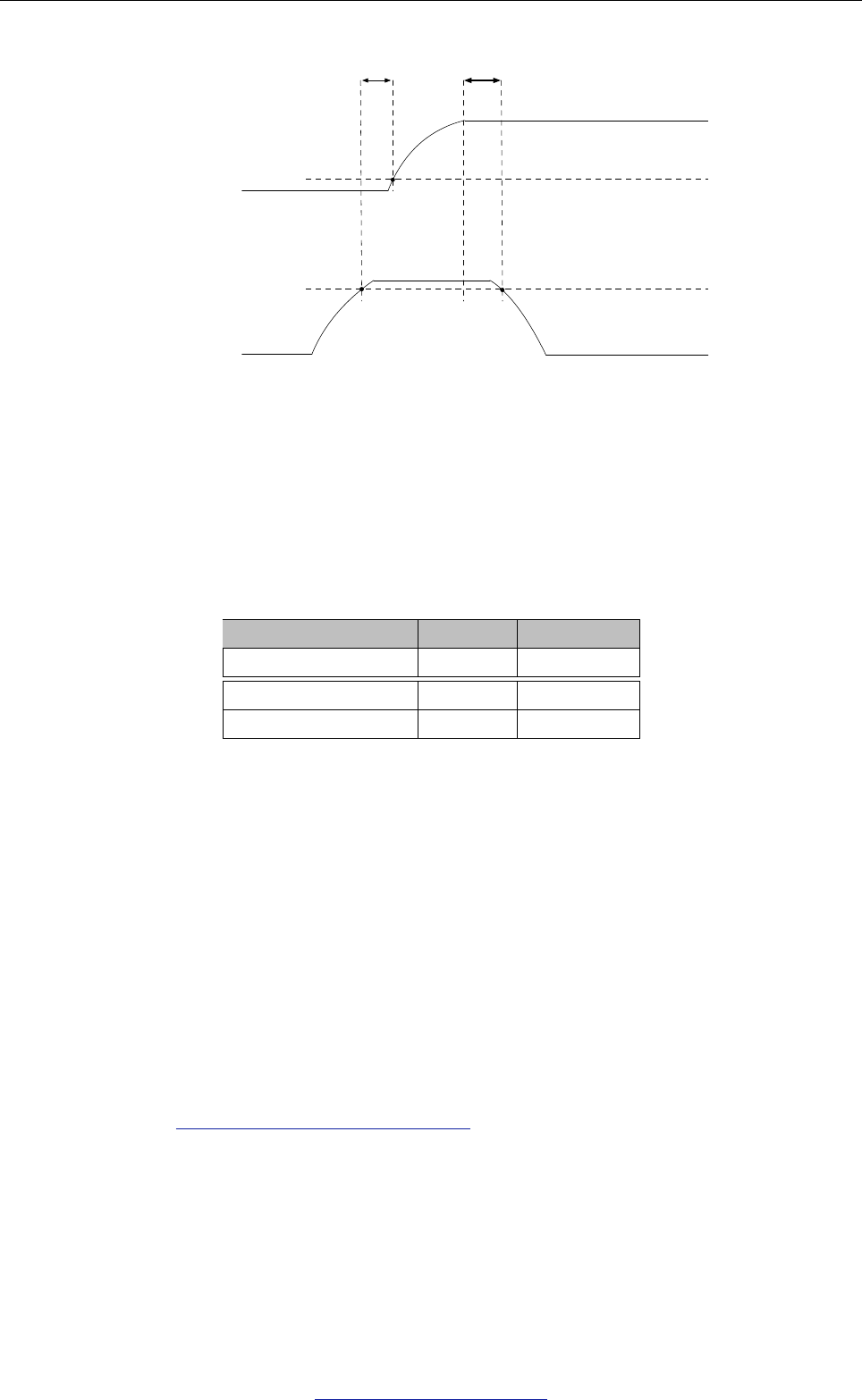
2.5.3 Chip Power-up and Reset
Once the power is supplied to the chip, its power rails need a short time to stabilize. After that, CHIP_PU – the
pin used for power-up and reset – is pulled high to activate the chip. For information on CHIP_PU as well as
power-up and reset timing, see Figure 2-3 and Table 2-8.
V
IL_nRST
t
ST BL
t
RST
2.8 V
VDDA,
VDD3P3,
VDD3P3_RTC,
VDD3P3_CPU
CHIP_PU
Figure 2-3. Visualization of Timing Parameters for Power-up and Reset
Table 2-8. Description of Timing Parameters for Power-up and Reset
Parameter Description Min (µs)
t
ST BL
Time reserved for the power rails of VDDA, VDD3P3, VDD3P3_RTC,
and VDD3P3_CPU to stabilize before the CHIP_PU pin is pulled
high to activate the chip
50
t
RST
Time reserved for CHIP_PU to stay below V
IL_nRST
to reset the
chip (see Table 4-4)
50
Espressif Systems 22
Submit Documentation Feedback
ESP32-S3 Series Datasheet v1.8

2 Pins
2.6 Strapping Pins
At each startup or reset, a chip requires some initial configuration parameters, such as in which boot mode to
load the chip, voltage of flash memory, etc. These parameters are passed over via the strapping pins. After reset,
the strapping pins operate as regular IO pins.
The parameters controlled by the given strapping pins at chip reset are as follows:
• Chip boot mode – GPIO0 and GPIO46
• VDD_SPI voltage – GPIO45
• ROM messages printing – GPIO46
• JTAG signal source – GPIO3
GPIO0, GPIO45, and GPIO46 are connected to the chip’s internal weak pull-up/pull-down resistors at chip reset.
These resistors determine the default bit values of the strapping pins. Also, these resistors determine the bit
values if the strapping pins are connected to an external high-impedance circuit.
Table 2-9. Default Configuration of Strapping Pins
Strapping Pin Default Configuration Bit Value
GPIO0 Pull-up 1
GPIO3 Floating –
GPIO45 Pull-down 0
GPIO46 Pull-down 0
To change the bit values, the strapping pins should be connected to external pull-down/pull-up resistances. If the
ESP32-S3 is used as a device by a host MCU, the strapping pin voltage levels can also be controlled by the host
MCU.
All strapping pins have latches. At system reset, the latches sample the bit values of their respective strapping
pins and store them until the chip is powered down or shut down. The states of latches cannot be changed in
any other way. It makes the strapping pin values available during the entire chip operation, and the pins are freed
up to be used as regular IO pins after reset.
Regarding the timing requirements for the strapping pins, there are such parameters as setup time and hold time.
For more information, see Table 2-10 and Figure 2-4.
Table 2-10. Description of Timing Parameters for the Strapping Pins
Parameter Description Min (ms)
t
SU
Setup time is the time reserved for the power rails to stabilize before
the CHIP_PU pin is pulled high to activate the chip.
0
t
H
Hold time is the time reserved for the chip to read the strapping pin
values after CHIP_PU is already high and before these pins start
operating as regular IO pins.
3
Espressif Systems 23
Submit Documentation Feedback
ESP32-S3 Series Datasheet v1.8
2 Pins
Strapping pin
VIL_nRST
VIH
t
SU
t
H
CHIP_PU
Figure 2-4. Visualization of Timing Parameters for the Strapping Pins
2.6.1 Chip Boot Mode Control
GPIO0 and GPIO46 control the boot mode after the reset is released. See Table 2-11 Chip Boot Mode
Control.
Table 2-11. Chip Boot Mode Control
Boot Mode GPIO0 GPIO46
Default Configuration 1 (Pull-up) 0 (Pull-down)
SPI Boot (default) 1 Any value
Joint Download Boot
1
0 0
1
Joint Download Boot mode supports the following
download methods:
• USB Download Boot:
– USB-Serial-JTAG Download Boot
– USB-OTG Download Boot
• UART Download Boot
In SPI Boot mode, the ROM bootloader loads and executes the program from SPI flash to boot the
system.
In Joint Download Boot mode, users can download binary files into flash using UART0 or USB interface. It is also
possible to download binary files into SRAM and execute it from SRAM.
In addition to SPI Boot and Joint Download Boot modes, ESP32-S3 also supports SPI Download Boot mode.
For details, please see ESP32-S3 Technical Reference Manual > Chapter Chip Boot Control.
2.6.2 VDD_SPI Voltage Control
The required VDD_SPI voltage for the chips of the ESP32-S3 Series can be found in Table 1-1
Comparison.
Depending on the value of EFUSE_VDD_SPI_FORCE, the voltage can be controlled in two ways.
Espressif Systems 24
Submit Documentation Feedback
ESP32-S3 Series Datasheet v1.8

2 Pins
Table 2-12. VDD_SPI Voltage Control
EFUSE_VDD_SPI_FORCE GPIO45 eFuse
1
Voltage VDD_SPI power source
2
0
0
Ignored
3.3 V VDD3P3_RTC via R
SP I
1 1.8 V Flash Voltage Regulator
1 Ignored
0 1.8 V Flash Voltage Regulator
1 3.3 V VDD3P3_RTC via R
SP I
1
eFuse: EFUSE_VDD_SPI_TIEH
2
See Section 2.5.2 Power Scheme
2.6.3 ROM Messages Printing Control
During boot process the messages by the ROM code can be printed to:
• (Default) UART and USB Serial/JTAG controller.
• USB Serial/JTAG controller.
• UART.
The ROM messages printing to UART or USB Serial/JTAG controller can be respectively disabled by configuring
registers and eFuse. For detailed information, please refer to ESP32-S3 Technical Reference Manual > Chapter
Chip Boot Control.
2.6.4 JTAG Signal Source Control
The strapping pin GPIO3 can be used to control the source of JTAG signals during the early boot process. This
pin does not have any internal pull resistors and the strapping value must be controlled by the external circuit that
cannot be in a high impedance state.
As Table 2-13 shows, GPIO3 is used in combination with EFUSE_DIS_PAD_JTAG, EFUSE_DIS_USB_JTAG, and
EFUSE_STRAP_JTAG_SEL.
Table 2-13. JTAG Signal Source Control
eFuse 1
a
eFuse 2
b
eFuse 3
c
GPIO3 JTAG Signal Source
0 0
0 Ignored USB Serial/JTAG Controller
1
0 JTAG pins MTDI, MTCK, MTMS, and MTDO
1 USB Serial/JTAG Controller
0 1 Ignored Ignored JTAG pins MTDI, MTCK, MTMS, and MTDO
1 0 Ignored Ignored USB Serial/JTAG Controller
1 1 Ignored Ignored JTAG is disabled
a
eFuse 1: EFUSE_DIS_PAD_JTAG
b
eFuse 2: EFUSE_DIS_USB_JTAG
c
eFuse 3: EFUSE_STRAP_JTAG_SEL
Espressif Systems 25
Submit Documentation Feedback
ESP32-S3 Series Datasheet v1.8

2 Pins
2.7 Pin Mapping Between Chip and Flash/PSRAM
Table 2-14 lists the pin mapping between the chip and flash/PSRAM for all SPI modes.
For chip variants with in-package flash/PSRAM (see Table 1-1 Comparison), the pins allocated for
communication with in-package flash/PSRAM can be identified depending on the SPI mode used.
For off-package flash/PSRAM, these are the recommended pin mappings.
For more information on SPI controllers, see also Section 3.5.2 Serial Peripheral Interface (SPI).
Notice:
It is not recommended to use the pins connected to flash/PSRAM for any other purposes.
Table 2-14. Pin Mapping Between Chip and In-package Flash/ PSRAM
Pin Pin Name Single SPI Dual SPI Quad SPI / QPI Octal SPI / OPI
No. Flash PSRAM Flash PSRAM Flash PSRAM Flash PSRAM
33 SPICLK CLK CLK CLK CLK CLK CLK CLK CLK
32 SPICS0
1
CS# CS# CS# CS#
28 SPICS1
2
CE# CE# CE# CE#
35 SPID DI SI/SIO0 DI SI/SIO0 DI SI/SIO0 DQ0 DQ0
34 SPIQ DO SO/SIO1 DO SO/SIO1 DO SO/SIO1 DQ1 DQ1
31 SPIWP WP# SIO2 WP# SIO2 WP# SIO2 DQ2 DQ2
30 SPIHD HOLD# SIO3 HOLD# SIO3 HOLD# SIO3 DQ3 DQ3
38 GPIO33 DQ4 DQ4
39 GPIO34 DQ5 DQ5
40 GPIO35 DQ6 DQ6
41 GPIO36 DQ7 DQ7
42 GPIO37 DQS/DM DQS/DM
1
CS0 is for in-package flash
2
CS1 is for in-package PSRAM
Espressif Systems 26
Submit Documentation Feedback
ESP32-S3 Series Datasheet v1.8

3 Functional Description
3 Functional Description
This chapter describes the functional modules of ESP32-S3.
3.1 CPU and Memory
3.1.1 CPU
ESP32-S3 has a low-power Xtensa
®
dual-core 32-bit LX7 microprocessor with the following features:
• Five-stage pipeline that supports the clock frequency of up to 240 MHz
• 16-bit/24-bit instruction set providing high code density
• 32-bit customized instruction set and 128-bit data bus that provide high computing performance
• Support for single-precision floating-point unit (FPU)
• 32-bit multiplier and 32-bit divider
• Unbuffered GPIO instructions
• 32 interrupts at six levels
• Windowed ABI with 64 physical general registers
• Trace function with TRAX compressor, up to 16 KB trace memory
• JTAG for debugging
For information about the Xtensa
®
Instruction Set Architecture, please refer to
Xtensa
®
Instruction Set Architecture (ISA) Summary.
3.1.2 Internal Memory
ESP32-S3’s internal memory includes:
• 384 KB ROM: for booting and core functions
• 512 KB on-chip SRAM: for data and instructions, running at a configurable frequency of up to 240 MHz
• RTC FAST memory: 8 KB SRAM that supports read/write/instruction fetch by the main CPU (LX7
dual-core processor). It can retain data in Deep-sleep mode
• RTC SLOW Memory: 8 KB SRAM that supports read/write/instruction fetch by the main CPU (LX7
dual-core processor) or coprocessors. It can retain data in Deep-sleep mode
• 4 Kbit eFuse: 1792 bits are reserved for user data, such as encryption key and device ID
• In-package flash and PSRAM: See details in Table 1-1 Comparison
3.1.3 External Flash and RAM
ESP32-S3 supports SPI, Dual SPI, Quad SPI, Octal SPI, QPI, and OPI interfaces that allow connection to
multiple external flash and RAM.
The external flash and RAM can be mapped into the CPU instruction memory space and read-only data memory
space. The external RAM can also be mapped into the CPU data memory space. ESP32-S3 supports up to 1
Espressif Systems 27
Submit Documentation Feedback
ESP32-S3 Series Datasheet v1.8
3 Functional Description
GB of external flash and RAM, and hardware encryption/decryption based on XTS-AES to protect users’
programs and data in flash and external RAM.
Through high-speed caches, ESP32-S3 can support at a time up to:
• External flash or RAM mapped into 32 MB instruction space as individual blocks of 64 KB
• External RAM mapped into 32 MB data space as individual blocks of 64 KB. 8-bit, 16-bit, 32-bit, and
128-bit reads and writes are supported. External flash can also be mapped into 32 MB data space as
individual blocks of 64 KB, but only supporting 8-bit, 16-bit, 32-bit and 128-bit reads.
Note:
After ESP32-S3 is initialized, firmware can customize the mapping of external RAM or flash into the CPU address space.
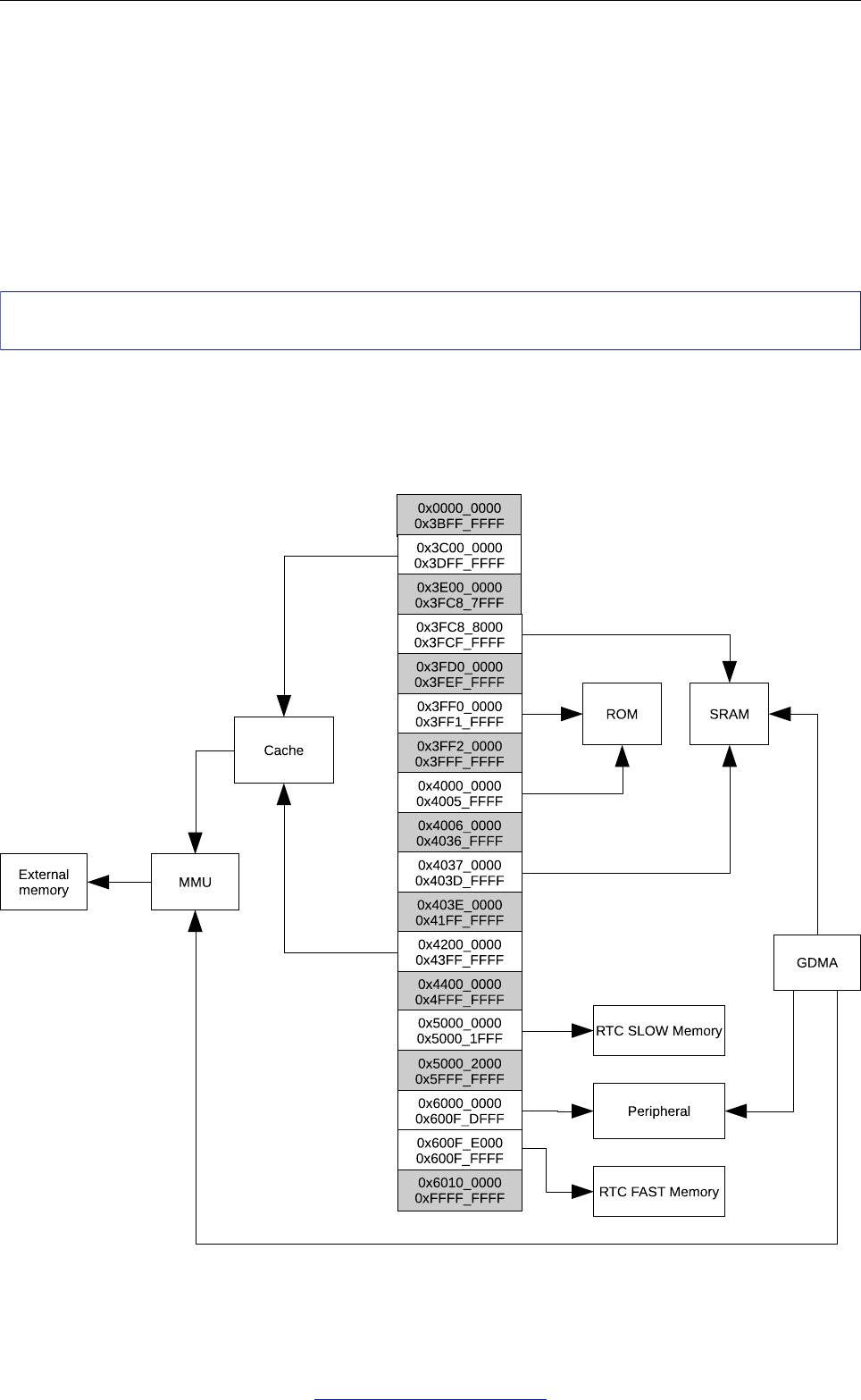
3.1.4 Address Mapping Structure
The address mapping structure of ESP32-S3 is shown below.
Figure 3-1. Address Mapping Structure
Espressif Systems 28
Submit Documentation Feedback
ESP32-S3 Series Datasheet v1.8

3 Functional Description
Note:
The memory space with gray background is not available to users.
3.1.5 Cache
ESP32-S3 has an instruction cache and a data cache shared by the two CPU cores. Each cache can be
partitioned into multiple banks and has the following features:
• Instruction cache: 16 KB (one bank) or 32 KB (two banks)
Data cache: 32 KB (one bank) or 64 KB (two banks)
• Instruction cache: four-way or eight-way set associative
Data cache: four-way set associative
• Block size of 16 bytes or 32 bytes for both instruction cache and data cache
• Pre-load function
• Lock function
• Critical word first and early restart
3.1.6 eFuse Controller
ESP32-S3 contains a 4-Kbit eFuse to store parameters, which are burned and read by an eFuse Controller. The
eFuse Controller has the following features:
• 4 Kbits in total, with 1792 bits reserved for users, e.g., encryption key and device ID
• One-time programmable storage
• Configurable write protection
• Configurable read protection
• Various hardware encoding schemes to protect against data corruption
For details, see ESP32-S3 Technical Reference Manual > Chapter eFuse Controller.
3.1.7 Processor Instruction Extensions
The ESP32-S3 contains a series of new extended instruction set in order to improve the operation efficiency of
specific AI and DSP (Digital Signal Processing) algorithms. The Processor Instruction Extensions (PIE) has the
following features:
• 128-bit new general-purpose registers
• 128-bit vector operations, e.g., complex multiplication, addition, subtraction, multiplication, shifting,
comparison, etc
• Data handling instructions and load/store operation instructions combined
• Non-aligned 128-bit vector data
• Saturation operation
Espressif Systems 29
Submit Documentation Feedback
ESP32-S3 Series Datasheet v1.8

3 Functional Description
3.2 RTC and Low-Power Management
3.2.1 Power Management Unit (PMU)
The ESP32-S3 has an advanced Power Management Unit (PMU). It can be flexibly configured to power up
different power domains of the chip to achieve the best balance between chip performance, power consumption,
and wakeup latency.
The integrated Ultra-Low-Power (ULP) coprocessors allow the ESP32-S3 to operate in Deep-sleep mode with
most of the power domains turned off, thus achieving extremely low-power consumption.
Configuring the PMU is a complex procedure. To simplify power management for typical scenarios, there are the
following predefined power modes that power up different combinations of power domains:
• Active mode – The CPU, RF circuits, and all peripherals are on. The chip can process data, receive,
transmit, and listen.
• Modem-sleep mode – The CPU is on, but the clock frequency can be reduced. The wireless connections
can be configured to remain active as RF circuits are periodically switched on when required.
• Light-sleep mode – The CPU stops running, and can be optionally powered on. The RTC peripherals, as
well as the ULP coprocessor can be woken up periodically by the timer. The chip can be woken up via all
wake up mechanisms: MAC, RTC timer, or external interrupts. Wireless connections can remain active.
Some groups of digital peripherals can be optionally powered off.
• Deep-sleep mode – Only RTC is powered on. Wireless connection data is stored in RTC memory.
For power consumption in different power modes, see Section 4.6 Current Consumption.
Figure 3-2 Components and Power Domains and the following Table 3-1 show the distribution of chip
components between power domains and power subdomains .
Espressif Systems 30
Submit Documentation Feedback
ESP32-S3 Series Datasheet v1.8

3 Functional Description
Wireless Digital Circuits
Wi-Fi MAC
Wi-Fi
Baseband
Bluetooth LE Link
Controller
Bluetooth LE
Baseband
Digital Power Domain
Espressif’s ESP32-S3 Wi-Fi + Bluetooth
®
Low Energy SoC
ROM SRAM
2.4 GHz Balun
+ Switch
2.4 GHz
Receiver
2.4 GHz
Transmitter
RF
Synthesizer
RF Circuits
Phase Lock
Loop
PLL
XTAL_CLK
External Main
Clock
RC_FAST_CLK
Fast RC
Oscillator
Analog Power Domain
Flash
Encryption
RNG
USB Serial/
JTAG
GPIO
UART
TWAI
®
General-
purpose
Timers
I2S
I2C
Pulse
Counter
LED PWM
Camera
Interface
SPI0/1
RMT
DIG ADC
System
Timer
LCD
Interface
Main System
Watchdog
Timers
MCPWM
RTC Memory
RTC
Watchdog
Timer
PMU
RTC Power Domain
RTC GPIO
Temperature
Sensor
Touch
Sensor
ULP
Coprocessor
RTC ADC
Optional RTC Peripherals
RTC I2C
eFuse
Controller
Power distribution
Power domain
Power subdomain
Super
Watchdog
CPU
Xtensa
®
Dual-
core 32-bit LX7
Microprocessor
JTAG
Cache
Interrupt
Matrix
World
Controller
Optional Digital Peripherals
RSA
Digital
Signature
SHA
AES
HMAC
Secure BootSPI2/3 GDMA
SD/MMC
Host
USB OTG
Figure 3-2. Components and Power Domains
Table 3-1. Components and Power Domains
RTC Digital Analog
Power
Mode
Power
Domain
Optional
RTC
Periph
CPU
Optional
Digital
Periph
Wireless
Digital
Circuits
RC_
FAST_
CLK
XTAL_
CLK
PLL
RF
Circuits
Active ON ON ON ON ON ON ON ON ON ON ON
Modem-sleep ON ON ON ON ON ON
1
ON ON ON ON OFF
2
Light-sleep ON ON ON OFF
1
ON
1
OFF
1
ON OFF OFF OFF OFF
2
Deep-sleep ON ON OFF OFF OFF OFF ON OFF OFF OFF OFF
1
Configurable, see ESP32-S3 Technical Reference Manual.
2
If Wireless Digital Circuits are on, RF circuits are periodically switched on when required by internal operation to keep active
wireless connections running.
Espressif Systems 31
Submit Documentation Feedback
ESP32-S3 Series Datasheet v1.8

3 Functional Description
3.2.2 Ultra-Low-Power Coprocessor
The ULP coprocessor is designed as a simplified, low-power replacement of CPU in sleep modes. It can be also
used to supplement the functions of the CPU in normal working mode. The ULP coprocessor and RTC memory
remain powered up during the Deep-sleep mode. Hence, the developer can store a program for the ULP
coprocessor in the RTC slow memory to access RTC GPIO, RTC peripheral devices, RTC timers and internal
sensors in Deep-sleep mode.
ESP32-S3 has two ULP coprocessors, one based on RISC-V instruction set architecture (ULP-RISC-V) and the
other on finite state machine (ULP-FSM). The clock of the coprocessors is the internal fast RC oscillator.
ULP-RISC-V has the following features:
• Support for RV32IMC instruction set
• Thirty-two 32-bit general-purpose registers
• 32-bit multiplier and divider
• Support for interrupts
• Booted by the CPU, its dedicated timer, or RTC GPIO
ULP-FSM has the following features:
• Support for common instructions including arithmetic, jump, and program control instructions
• Support for on-board sensor measurement instructions
• Booted by the CPU, its dedicated timer, or RTC GPIO
Note that these two coprocessors cannot work simultaneously.
3.3 Analog Peripherals
3.3.1 Analog-to-Digital Converter (ADC)
ESP32-S3 integrates two 12-bit SAR ADCs and supports measurements on 20 channels (analog-enabled pins).
For power-saving purpose, the ULP coprocessors in ESP32-S3 can also be used to measure voltage in sleep
modes. By using threshold settings or other methods, we can awaken the CPU from sleep modes.
3.3.2 Temperature Sensor
The temperature sensor generates a voltage that varies with temperature. The voltage is internally converted via
an ADC into a digital value.
The temperature sensor has a range of 20 °C to 110 °C. It is designed primarily to sense the temperature
changes inside the chip. The temperature value depends on factors such as microcontroller clock frequency or
I/O load. Generally, the chip’s internal temperature is higher than the ambient temperature.
3.3.3 Touch Sensor
ESP32-S3 has 14 capacitive-sensing GPIOs, which detect variations induced by touching or approaching the
GPIOs with a finger or other objects. The low-noise nature of the design and the high sensitivity of the circuit
allow relatively small pads to be used. Arrays of pads can also be used, so that a larger area or more points can
Espressif Systems 32
Submit Documentation Feedback
ESP32-S3 Series Datasheet v1.8

3 Functional Description
be detected. The touch sensing performance can be further enhanced by the waterproof design and digital
filtering feature.
Note:
ESP32-S3 Touch Sensor has not passed the Conducted Susceptibility (CS) test for now, and thus has limited application
scenarios.
3.4 System Components
3.4.1 Reset and Clock
ESP32-S3 provides four reset levels, namely CPU Reset, Core Reset, System Reset, and Chip Reset.
• Support four reset levels:
– CPU Reset: only resets CPUx core. CPUx can be CPU0 or CPU1 here. Once such reset is released,
programs will be executed from CPUx reset vector. Each CPU core has its own reset logic. If CPU
Reset is from CPU0, the sensitive registers will be reset, too.
– Core Reset: resets the whole digital system except RTC, including CPU0, CPU1, peripherals, Wi-Fi,
Bluetooth
®
LE (BLE), and digital GPIOs.
– System Reset: resets the whole digital system, including RTC.
– Chip Reset: resets the whole chip.
• Support software reset and hardware reset:
– Software reset is triggered by CPUx configuring its corresponding registers.
– Hardware reset is directly triggered by the circuit.
For details, see ESP32-S3 Technical Reference Manual > Chapter Reset and Clock.
3.4.2 Interrupt Matrix
The interrupt matrix embedded in ESP32-S3 independently allocates peripheral interrupt sources to the two
CPUs’ peripheral interrupts, to timely inform CPU0 or CPU1 to process the interrupts once the interrupt signals
are generated. The Interrupt Matrix has the following features:
• 99 peripheral interrupt sources as input
• Generate 26 peripheral interrupts to CPU0 and 26 peripheral interrupts to CPU1 as output. Note that the
remaining six CPU0 interrupts and six CPU1 interrupts are internal interrupts.
• Disable CPU non-maskable interrupt (NMI) sources
• Query current interrupt status of peripheral interrupt sources
For details, see ESP32-S3 Technical Reference Manual > Chapter Interrupt Matrix.
3.4.3 Permission Control
In ESP32-S3, the Permission Control module is used to control access to the slaves (including internal memory,
peripherals, external flash and RAM). The host can access its slave only if it has the right permission. In this way,
data and instructions are protected from illegitimate read or write.
Espressif Systems 33
Submit Documentation Feedback
ESP32-S3 Series Datasheet v1.8

3 Functional Description
The ESP32-S3 CPU can run in both Secure World and Non-secure World where independent permission
controls are adopted. The Permission Control module is able to identify which World the host is running and then
proceed with its normal operations.
The Permission Control module has the following features:
• Manage access to internal memory by:
– CPU
– CPU trace module
– GDMA
• Manage access to external flash and RAM by:
– MMU
– SPI1
– GDMA
– CPU through Cache
• Manage access to peripherals, supporting
– independent permission control for each peripheral
– monitoring non-aligned access
– access control for customized address range
• Integrate permission lock register
– All permission registers can be locked with the permission lock register. Once locked, the permission
register and the lock register cannot be modified, unless the CPU is reset.
• Integrate permission monitor interrupt
– In case of illegitimate access, the permission monitor interrupt will be triggered and the CPU will be
informed to handle the interrupt.
3.4.4 System Registers
ESP32-S3 system registers can be used to control the following peripheral blocks and core modules:
• System and memory
• Clock
• Software Interrupt
• Low-power management
• Peripheral clock gating and reset
• CPU Control
For details, see ESP32-S3 Technical Reference Manual > Chapter System Registers.
Espressif Systems 34
Submit Documentation Feedback
ESP32-S3 Series Datasheet v1.8

3 Functional Description
3.4.5 GDMA Controller
ESP32-S3 has a general-purpose DMA controller (GDMA) with five independent channels for transmitting and
another five independent channels for receiving. These ten channels are shared by peripherals that have DMA
feature, and support dynamic priority.
The DMA controller controls data transfer using linked lists. It allows peripheral-to-memory and
memory-to-memory data transfer at a high speed. All channels can access internal and external RAM.
The ten peripherals on ESP32-S3 with DMA feature are SPI2, SPI3, UHCI0, I2S0, I2S1, LCD/CAM, AES, SHA,
ADC, and RMT.
For details, see ESP32-S3 Technical Reference Manual > Chapter GDMA Controller.
3.4.6 CPU Clock
The CPU clock has three possible sources:
• External main crystal clock
• Internal fast RC oscillator (typically about 17.5 MHz, and adjustable)
• PLL clock
The application can select the clock source from the three clocks above. The selected clock source drives the
CPU clock directly, or after division, depending on the application. Once the CPU is reset, the default clock
source would be the external main crystal clock divided by 2.
Note:
ESP32-S3 is unable to operate without an external main crystal clock.
For details about clocks, see ESP32-S3 Technical Reference Manual > Chapter Reset and Clock.
3.4.7 RTC Clock
The RTC slow clock is used for RTC counter, RTC watchdog and low-power controller. It has three possible
sources:
• External low-speed (32 kHz) crystal clock
• Internal slow RC oscillator (typically about 136 kHz, and adjustable)
• Internal fast RC oscillator divided clock (derived from the internal fast RC oscillator divided by 256)
The RTC fast clock is used for RTC peripherals and sensor controllers. It has two possible sources:
• External main crystal clock divided by 2
• Internal fast RC oscillator (typically about 17.5 MHz, and adjustable)
3.4.8 Clock Glitch Detection
The Clock Glitch Detection module on ESP32-S3 monitors input clock signals from XTAL_CLK. If it detects a
glitch with a width shorter than 3 ns, input clock signals from XTAL_CLK are blocked.
For details, see ESP32-S3 Technical Reference Manual > Chapter Clock Glitch Detection.
Espressif Systems 35
Submit Documentation Feedback
ESP32-S3 Series Datasheet v1.8

3 Functional Description
3.5 Digital Peripherals
3.5.1 IO MUX and GPIO Matrix
GPIO Matrix Features
• A full-switching matrix between the peripheral input/output signals and the GPIO pins
• 175 digital peripheral input signals can be sourced from the input of any GPIO pins
• The output of any GPIO pins can be from any of the 184 digital peripheral output signals
• Supports signal synchronization for peripheral inputs based on APB clock bus
• Provides input signal filter
• Supports sigma delta modulated output
• Supports GPIO simple input and output
IO MUX Features
• Provides one configuration register IO_MUX_GPIOn_REG for each GPIO pin. The pin can be configured to
– perform GPIO function routed by GPIO matrix.
– or perform direct connection bypassing GPIO matrix.
• Supports some high-speed digital signals (SPI, JTAG, UART) bypassing GPIO matrix for better
high-frequency digital performance. In this case, IO MUX is used to connect these pins directly to
peripherals.
RTC IO MUX Features
• Controls low power feature of 22 RTC GPIO pins.
• Controls analog functions of 22 RTC GPIO pins.
• Redirects 22 RTC input/output signals to RTC system.
For details, see ESP32-S3 Technical Reference Manual > Chapter IO MUX and GPIO Matrix.
3.5.2 Serial Peripheral Interface (SPI)
ESP32-S3 has the following SPI interfaces:
• SPI0 used by ESP32-S3’s GDMA controller and cache to access in-package or off-package flash/PSRAM
• SPI1 used by the CPU to access in-package or off-package flash/PSRAM
• SPI2 is a general purpose SPI controller with access to a DMA channel allocated by the GDMA controller
• SPI3 is a general purpose SPI controller with access to a DMA channel allocated by the GDMA controller
Features of SPI0 and SPI1
• Supports Single SPI, Dual SPI, Quad SPI, Octal SPI, QPI, and OPI modes
• 8-line SPI mode supports single data rate (SDR) and double data rate (DDR)
• Configurable clock frequency with a maximum of 120 MHz for 8-line SPI SDR/DDR modes
Espressif Systems 36
Submit Documentation Feedback
ESP32-S3 Series Datasheet v1.8

3 Functional Description
• Data transmission is in bytes
Features of SPI2
• Supports operation as a master or slave
• Connects to a DMA channel allocated by the GDMA controller
• Supports Single SPI, Dual SPI, Quad SPI, Octal SPI, QPI, and OPI modes
• Configurable clock polarity (CPOL) and phase (CPHA)
• Configurable clock frequency
• Data transmission is in bytes
• Configurable read and write data bit order: most-significant bit (MSB) first, or least-significant bit (LSB) first
• As a master
– Supports 2-line full-duplex communication with clock frequency up to 80 MHz
– Full-duplex 8-line SPI mode supports single data rate (SDR) only
– Supports 1-, 2-, 4-, 8-line half-duplex communication with clock frequency up to 80 MHz
– Half-duplex 8-line SPI mode supports both single data rate (up to 80 MHz) and double data rate (up to
40 MHz)
– Provides six SPI_CS pins for connection with six independent SPI slaves
– Configurable CS setup time and hold time
• As a slave
– Supports 2-line full-duplex communication with clock frequency up to 60 MHz
– Supports 1-, 2-, 4-line half-duplex communication with clock frequency up to 60 MHz
– Full-duplex and half-duplex 8-line SPI mode supports single data rate (SDR) only
Features of SPI3
• Supports operation as a master or slave
• Connects to a DMA channel allocated by the GDMA controller
• Supports Single SPI, Dual SPI, Quad SPI, and QPI modes
• Configurable clock polarity (CPOL) and phase (CPHA)
• Configurable clock frequency
• Data transmission is in bytes
• Configurable read and write data bit order: most-significant bit (MSB) first, or least-significant bit (LSB) first
• As a master
– Supports 2-line full-duplex communication with clock frequency up to 80 MHz
– Supports 1-, 2-, 4-line half-duplex communication with clock frequency up to 80 MHz
Espressif Systems 37
Submit Documentation Feedback
ESP32-S3 Series Datasheet v1.8

3 Functional Description
– Provides three SPI_CS pins for connection with three independent SPI slaves
– Configurable CS setup time and hold time
• As a slave
– Supports 2-line full-duplex communication with clock frequency up to 60 MHz
– Supports 1-, 2-, 4-line half-duplex communication with clock frequency up to 60 MHz
Pin Configuration
Table 3-2. SPI Pin Configuration
Interface Suggested IO MUX Pins Routing via GPIO Matrix
SPI0/1 See Table 2-3 IO MUX and GPIO Pin Functions, notes 5c, 5d –
SPI2 See Table 2-3 IO MUX and GPIO Pin Functions, note 5e Any IO pins
SPI3 – Any IO pins
For details, see ESP32-S3 Technical Reference Manual > Chapter SPI Controller.
3.5.3 LCD Interface
ESP32-S3 supports 8-bit ~16-bit parallel RGB, I8080, and MOTO6800 interfaces. These interfaces operate at
40 MHz or lower, and support conversion among RGB565, YUV422, YUV420, and YUV411.
3.5.4 Camera Interface
ESP32-S3 supports an 8-bit ~16-bit DVP image sensor, with clock frequency of up to 40 MHz. The camera
interface supports conversion among RGB565, YUV422, YUV420, and YUV411.
3.5.5 UART Controller
ESP32-S3 has three UART (Universal Asynchronous Receiver Transmitter) controllers, i.e., UART0, UART1, and
UART2, which support IrDA and asynchronous communication (RS232 and RS485) at a speed of up to 5 Mbps.
Each UART Controller has the following features:
• Three clock sources that can be divided
• Programmable baud rate
• 1024 x 8-bit RAM shared by TX FIFOs and RX FIFOs of the three UART controllers
• Full-duplex asynchronous communication
• Automatic baud rate detection of input signals
• Data bits ranging from 5 to 8
• Stop bits of 1, 1.5, 2 or 3 bits
• Parity bit
• Special character AT_CMD detection
• RS485 protocol
Espressif Systems 38
Submit Documentation Feedback
ESP32-S3 Series Datasheet v1.8

3 Functional Description
• IrDA protocol
• High-speed data communication using GDMA
• UART as wake-up source
• Software and hardware flow control
For details, see ESP32-S3 Technical Reference Manual > Chapter UART Controller.
3.5.6 I2C Interface
ESP32-S3 has two I2C bus interfaces which are used for I2C master mode or slave mode, depending on the
user’s configuration. The I2C interfaces support:
• Standard mode (100 kbit/s)
• Fast mode (400 kbit/s)
• Up to 800 kbit/s (constrained by SCL and SDA pull-up strength)
• 7-bit and 10-bit addressing mode
• Double addressing mode (slave addressing and slave register addressing)
The hardware provides a command abstraction layer to simplify the usage of the I2C peripheral.
For details, see ESP32-S3 Technical Reference Manual > Chapter I2C Controller.
3.5.7 I2S Interface
ESP32-S3 includes two standard I2S interfaces. They can operate in master mode or slave mode, in full-duplex
mode or half-duplex communication mode, and can be configured to operate with an 8-bit, 16-bit, 24-bit, or
32-bit resolution as an input or output channel. BCK clock frequency, from 10 kHz up to 40 MHz, is
supported.
The I2S interface has a dedicated DMA controller. It supports TDM PCM, TDM MSB alignment, TDM LSB
alignment, TDM Phillips, and PDM interface.
3.5.8 Remote Control Peripheral
The RMT (Remote Control Peripheral) module is designed to send and receive infrared remote control signals. It
has the following features:
• Four TX channels
• Four RX channels
• Support multiple channels (programmable) transmitting data simultaneously
• Eight channels share a 384 x 32-bit RAM
• Support modulation on TX pulses
• Support filtering and demodulation on RX pulses
• Wrap TX mode
• Wrap RX mode
Espressif Systems 39
Submit Documentation Feedback
ESP32-S3 Series Datasheet v1.8

3 Functional Description
• Continuous TX mode
• DMA access for TX mode on channel 3
• DMA access for RX mode on channel 7
For details, see ESP32-S3 Technical Reference Manual > Chapter Remote Control Peripheral.
3.5.9 Pulse Count Controller
The pulse count controller captures pulse and counts pulse edges through multiple modes. It has the following
features:
• Four independent pulse counters (units) that count from 1 to 65535
• Each unit consists of two independent channels sharing one pulse counter
• All channels have input pulse signals (e.g. sig_ch0_un) with their corresponding control signals (e.g.
ctrl_ch0_un)
• Independently filter glitches of input pulse signals (sig_ch0_un and sig_ch1_un) and control signals
(ctrl_ch0_un and ctrl_ch1_un) on each unit
• Each channel has the following parameters:
1. Selection between counting on positive or negative edges of the input pulse signal
2. Configuration to Increment, Decrement, or Disable counter mode for control signal’s high and low
states
For details, see ESP32-S3 Technical Reference Manual > Chapter Pulse Count Controller.
3.5.10 LED PWM Controller
The LED PWM controller can generate independent digital waveforms on eight channels. The LED PWM
controller has the following features:
• Can generate a digital waveform with configurable periods and duty cycle. The duty cycle resolution can be
up to 14 bits within a 1 ms period.
• Has multiple clock sources, including APB clock and external main crystal clock.
• Can operate when the CPU is in Light-sleep mode.
• Supports gradual increase or decrease of duty cycle, which is useful for the LED RGB color-fading
generator.
For details, see ESP32-S3 Technical Reference Manual > Chapter LED PWM Controller.
3.5.11 USB 2.0 OTG Full-Speed Interface
ESP32-S3 features a full-speed USB OTG interface along with an integrated transceiver. The USB OTG interface
complies with the USB 2.0 specification. It has the following features:
General Features
• FS and LS data rates
• HNP and SRP as A-device or B-device
Espressif Systems 40
Submit Documentation Feedback
ESP32-S3 Series Datasheet v1.8

3 Functional Description
• Dynamic FIFO (DFIFO) sizing
• Multiple modes of memory access
– Scatter/Gather DMA mode
– Buffer DMA mode
– Slave mode
• Can choose integrated transceiver or external transceiver
• Utilizing integrated transceiver with USB Serial/JTAG by time-division multiplexing when only integrated
transceiver is used
• Support USB OTG using one of the transceivers while USB Serial/JTAG using the other one when both
integrated transceiver or external transceiver are used
Device Mode Features
• Endpoint number 0 always present (bi-directional, consisting of EP0 IN and EP0 OUT)
• Six additional endpoints (endpoint numbers 1 to 6), configurable as IN or OUT
• Maximum of five IN endpoints concurrently active at any time (including EP0 IN)
• All OUT endpoints share a single RX FIFO
• Each IN endpoint has a dedicated TX FIFO
Host Mode Features
• 8 channels (pipes)
– A control pipe consists of two channels (IN and OUT), as IN and OUT transactions must be handled
separately. Only Control transfer type is supported.
– Each of the other seven channels is dynamically configurable to be IN or OUT, and supports Bulk,
Isochronous, and Interrupt transfer types.
• All channels share an RX FIFO, non-periodic TX FIFO, and periodic TX FIFO. The size of each FIFO is
configurable.
For details, see ESP32-S3 Technical Reference Manual > Chapter USB On-The-Go.
3.5.12 USB Serial/JTAG Controller
ESP32-S3 integrates a USB Serial/JTAG controller that supports the following features:
• USB Full-speed device.
• Can be configured to either use internal USB PHY of ESP32-S3 or external PHY via GPIO matrix.
• Fixed function device, hardwired for CDC-ACM (Communication Device Class - Abstract Control Model)
and JTAG adapter functionality.
• 2 OUT Endpoints, 3 IN Endpoints in addition to Control Endpoint 0; Up to 64-byte data payload size.
• Internal PHY, so no or very few external components needed to connect to a host computer.
• CDC-ACM adherent serial port emulation is plug-and-play on most modern OSes.
Espressif Systems 41
Submit Documentation Feedback
ESP32-S3 Series Datasheet v1.8

3 Functional Description
• JTAG interface allows fast communication with CPU debug core using a compact representation of JTAG
instructions.
• CDC-ACM supports host controllable chip reset and entry into download mode.
For details, see ESP32-S3 Technical Reference Manual > Chapter USB Serial/JTAG Controller.
3.5.13 Motor Control PWM (MCPWM)
ESP32-S3 integrates two MCPWM that can be used to drive digital motors and smart light. Each MCPWM
peripheral has one clock divider (prescaler), three PWM timers, three PWM operators, and a capture module.
PWM timers are used for generating timing references. The PWM operators generate desired waveform based
on the timing references. Any PWM operator can be configured to use the timing references of any PWM timers.
Different PWM operators can use the same PWM timer s timing references to produce related PWM signals.
PWM operators can also use different PWM timers values to produce the PWM signals that work alone.
Different PWM timers can also be synchronized together.
For details, see ESP32-S3 Technical Reference Manual > Chapter Motor Control PWM.
3.5.14 SD/MMC Host Controller
ESP32-S3 has an SD/MMC Host Controller with the following features:
• Secure Digital (SD) memory version 3.0 and version 3.01
• Secure Digital I/O (SDIO) version 3.0
• Consumer Electronics Advanced Transport Architecture (CE-ATA) version 1.1
• Multimedia Cards (MMC version 4.41, eMMC version 4.5 and version 4.51)
• Up to 80 MHz clock output
• Three data bus modes:
– 1-bit
– 4-bit (supports two SD/SDIO/MMC 4.41 cards, and one SD card operating at 1.8 V in 4-bit mode)
– 8-bit
For details, see ESP32-S3 Technical Reference Manual > Chapter SD/MMC Host Controller.
3.5.15 TWAI
®
Controller
The Two-wire Automotive Interface (TWAI) is a multi-master, multi-cast communication protocol with error
detection and signaling as well as inbuilt message priorities and arbitration. The TWAI controller in ESP32-S3
supports the following features:
• Compatible with ISO 11898-1 protocol (CAN Specification 2.0)
• Standard frame format (11-bit ID) and extended frame format (29-bit ID)
• Bit rates from 1 Kbit/s to 1 Mbit/s
• Multiple modes of operation:
– Normal
Espressif Systems 42
Submit Documentation Feedback
ESP32-S3 Series Datasheet v1.8

3 Functional Description
– Listen Only
– Self-Test (no acknowledgment required)
• 64-byte receive FIFO
• Acceptance filter (single and dual filter modes)
• Error detection and handling:
– Error counters
– Configurable error interrupt threshold
– Error code capture
– Arbitration lost capture
For details, see ESP32-S3 Technical Reference Manual > Chapter Two-wire Automotive Interface.
3.6 Radio and Wi-Fi
The ESP32-S3 radio consists of the following blocks:
• 2.4 GHz receiver
• 2.4 GHz transmitter
• Bias and regulators
• Balun and transmit-receive switch
• Clock generator
3.6.1 2.4 GHz Receiver
The 2.4 GHz receiver demodulates the 2.4 GHz RF signal to quadrature baseband signals and converts them to
the digital domain with two high-resolution, high-speed ADCs. To adapt to varying signal channel conditions,
ESP32-S3 integrates RF filters, Automatic Gain Control (AGC), DC offset cancelation circuits, and baseband
filters.
3.6.2 2.4 GHz Transmitter
The 2.4 GHz transmitter modulates the quadrature baseband signals to the 2.4 GHz RF signal, and drives the
antenna with a high-powered CMOS power amplifier. The use of digital calibration further improves the linearity of
the power amplifier.
To compensate for receiver imperfections, additional calibration methods are built into the chip, including:
• Carrier leakage compensation
• I/Q amplitude/phase matching
• Baseband nonlinearities suppression
• RF nonlinearities suppression
• Antenna matching
Espressif Systems 43
Submit Documentation Feedback
ESP32-S3 Series Datasheet v1.8

3 Functional Description
These built-in calibration routines reduce the cost and time to the market for your product, and eliminate the need
for specialized testing equipment.
3.6.3 Clock Generator
The clock generator produces quadrature clock signals of 2.4 GHz for both the receiver and the transmitter. All
components of the clock generator are integrated into the chip, including inductors, varactors, filters, regulators,
and dividers.
The clock generator has built-in calibration and self-test circuits. Quadrature clock phases and phase noise are
optimized on chip with patented calibration algorithms which ensure the best performance of the receiver and the
transmitter.
3.6.4 Wi-Fi Radio and Baseband
The ESP32-S3 Wi-Fi radio and baseband support the following features:
• 802.11b/g/n
• 802.11n MCS0-7 that supports 20 MHz and 40 MHz bandwidth
• 802.11n MCS32
• 802.11n 0.4 µs guard-interval
• Data rate up to 150 Mbps
• RX STBC (single spatial stream)
• Adjustable transmitting power
• Antenna diversity:
ESP32-S3 supports antenna diversity with an external RF switch. This switch is controlled by one or more
GPIOs, and used to select the best antenna to minimize the effects of channel imperfections.
3.6.5 Wi-Fi MAC
ESP32-S3 implements the full 802.11b/g/n Wi-Fi MAC protocol. It supports the Basic Service Set (BSS) STA and
SoftAP operations under the Distributed Control Function (DCF). Power management is handled automatically
with minimal host interaction to minimize the active duty period.
The ESP32-S3 Wi-Fi MAC applies the following low-level protocol functions automatically:
• 4 × virtual Wi-Fi interfaces
• Simultaneous Infrastructure BSS Station mode, SoftAP mode, and Station + SoftAP mode
• RTS protection, CTS protection, Immediate Block ACK
• Fragmentation and defragmentation
• TX/RX A-MPDU, TX/RX A-MSDU
• TXOP
• WMM
• GCMP, CCMP, TKIP, WAPI, WEP, and BIP
Espressif Systems 44
Submit Documentation Feedback
ESP32-S3 Series Datasheet v1.8

3 Functional Description
• Automatic beacon monitoring (hardware TSF)
• 802.11mc FTM
3.6.6 Networking Features
Users are provided with libraries for TCP/IP networking, ESP-WIFI-MESH networking, and other networking
protocols over Wi-Fi. TLS 1.2 support is also provided.
3.7 Bluetooth LE
ESP32-S3 includes a Bluetooth Low Energy subsystem that integrates a hardware link layer controller, an
RF/modem block and a feature-rich software protocol stack. It supports the core features of Bluetooth 5 and
Bluetooth mesh.
3.7.1 Bluetooth LE Radio and PHY
Bluetooth Low Energy radio and PHY in ESP32-S3 support:
• 1 Mbps PHY
• 2 Mbps PHY for high transmission speed and high data throughput
• Coded PHY for high RX sensitivity and long range (125 Kbps and 500 Kbps)
• Class 1 transmit power without external PA
• HW Listen before talk (LBT)
3.7.2 Bluetooth LE Link Layer Controller
Bluetooth Low Energy Link Layer Controller in ESP32-S3 supports:
• LE advertising extensions, to enhance broadcasting capacity and broadcast more intelligent data
• Multiple advertisement sets
• Simultaneous advertising and scanning
• Multiple connections in simultaneous central and peripheral roles
• Adaptive frequency hopping and channel assessment
• LE channel selection algorithm #2
• Connection parameter update
• High duty cycle non-connectable advertising
• LE privacy 1.2
• LE data packet length extension
• Link layer extended scanner filter policies
• Low duty cycle directed advertising
• Link layer encryption
• LE Ping
Espressif Systems 45
Submit Documentation Feedback
ESP32-S3 Series Datasheet v1.8

3 Functional Description
3.8 Timers and Watchdogs
3.8.1 General Purpose Timers
ESP32-S3 is embedded with four 54-bit general-purpose timers, which are based on 16-bit prescalers and
54-bit auto-reload-capable up/down-timers.
The timers’ features are summarized as follows:
• A 16-bit clock prescaler, from 2 to 65536
• A 54-bit time-base counter programmable to be incrementing or decrementing
• Able to read real-time value of the time-base counter
• Halting and resuming the time-base counter
• Programmable alarm generation
• Timer value reload (Auto-reload at alarm or software-controlled instant reload)
• Level interrupt generation
For details, see ESP32-S3 Technical Reference Manual > Chapter Timer Group.
3.8.2 System Timer
ESP32-S3 integrates a 52-bit system timer, which has two 52-bit counters and three comparators. The system
timer has the following features:
• Counters with a clock frequency of 16 MHz
• Three types of independent interrupts generated according to alarm value
• Two alarm modes: target mode and period mode
• 52-bit target alarm value and 26-bit periodic alarm value
• Read sleep time from RTC timer when the chip is awaken from Deep-sleep or Light-sleep mode
• Counters can be stalled if the CPU is stalled or in OCD mode
For details, see ESP32-S3 Technical Reference Manual > Chapter System Timer.
3.8.3 Watchdog Timers
The ESP32-S3 contains three watchdog timers: one in each of the two timer groups (called Main System
Watchdog Timers, or MWDT) and one in the RTC Module (called the RTC Watchdog Timer, or RWDT).
During the flash boot process, RWDT and the first MWDT are enabled automatically in order to detect and
recover from booting errors.
Watchdog timers have the following features:
• Four stages, each with a programmable timeout value. Each stage can be configured, enabled and
disabled separately
• Interrupt, CPU reset, or core reset for MWDT upon expiry of each stage; interrupt, CPU reset, core reset, or
system reset for RWDT upon expiry of each stage
Espressif Systems 46
Submit Documentation Feedback
ESP32-S3 Series Datasheet v1.8

3 Functional Description
• 32-bit expiry counter
• Write protection, to prevent RWDT and MWDT configuration from being altered inadvertently
• Flash boot protection
If the boot process from an SPI flash does not complete within a predetermined period of time, the
watchdog will reboot the entire main system.
For details, see ESP32-S3 Technical Reference Manual > Chapter Watchdog Timers.
3.8.4 XTAL32K Watchdog Timers
Interrupt and Wake-Up
When the XTAL32K watchdog timer detects the oscillation failure of XTAL32K_CLK, an oscillation failure interrupt
RTC_XTAL32K_DEAD_INT (for interrupt description, please refer to ESP32-S3 Technical Reference Manual) is
generated. At this point, the CPU will be woken up if in Light-sleep mode or Deep-sleep mode.
BACKUP32K_CLK
Once the XTAL32K watchdog timer detects the oscillation failure of XTAL32K_CLK, it replaces XTAL32K_CLK
with BACKUP32K_CLK (with a frequency of 32 kHz or so) derived from RTC_CLK as RTC s SLOW_CLK, so as
to ensure proper functioning of the system.
For details, see ESP32-S3 Technical Reference Manual > Chapter XTAL32K Watchdog Timers.
3.9 Cryptography/Security Components
3.9.1 External Memory Encryption and Decryption
ESP32-S3 integrates an External Memory Encryption and Decryption module that complies with the XTS-AES
standard. It supports the following features:
• General XTS-AES algorithm, compliant with IEEE Std 1619-2007
• Software-based manual encryption
• High-speed auto encryption, without software’s participation
• High-speed auto decryption, without software’s participation
• Encryption and decryption functions jointly determined by registers configuration, eFuse parameters, and
boot mode
For details, see ESP32-S3 Technical Reference Manual > Chapter External Memory Encryption and Decryption.
3.9.2 Secure Boot
Secure Boot feature uses a hardware root of trust to ensure only signed firmware (with RSA-PSS signature) can
be booted.
3.9.3 HMAC Accelerator
The Hash-based Message Authentication Code (HMAC) module computes Message Authentication Codes
(MACs) using Hash algorithm and keys as described in RFC 2104. The HMAC Accelerator in ESP32-S3 supports
Espressif Systems 47
Submit Documentation Feedback
ESP32-S3 Series Datasheet v1.8

3 Functional Description
the following features:
• Standard HMAC-SHA-256 algorithm
• Hash result only accessible by configurable hardware peripheral (in downstream mode)
• Compatible to challenge-response authentication algorithm
• Generates required keys for the Digital Signature (DS) peripheral (in downstream mode)
• Re-enables soft-disabled JTAG (in downstream mode)
For details, see ESP32-S3 Technical Reference Manual > Chapter HMAC Accelerator.
3.9.4 Digital Signature
A Digital Signature is used to verify the authenticity and integrity of a message using a cryptographic algorithm.
The Digital Signature (DS) in ESP32-S3 supports the following features:
• RSA Digital Signatures with key length up to 4096 bits
• Encrypted private key data, only decryptable by DS peripheral
• SHA-256 digest to protect private key data against tampering by an attacker
For details, see ESP32-S3 Technical Reference Manual > Chapter Digital Signature.
3.9.5 World Controller
The ESP32-S3 can divide the hardware and software resources into a Secure World and a Non-Secure World to
prevent sabotage or access to device information. Switching between the two worlds is performed by the World
Controller, which supports the following features:
• Control of the CPU switching between secure and non-secure worlds
• Control of 15 DMA peripherals switching between secure and non-secure worlds
• Record of CPU’s world switching logs
• Shielding of the CPU’s NMI interrupt
3.9.6 SHA Accelerator
ESP32-S3 integrates an SHA accelerator, which is a hardware device that speeds up SHA algorithm significantly.
The SHA Accelerator supports the following features:
• All the hash algorithms introduced in FIPS PUB 180-4 Spec.
– SHA-1
– SHA-224
– SHA-256
– SHA-384
– SHA-512
– SHA-512/224
– SHA-512/256
Espressif Systems 48
Submit Documentation Feedback
ESP32-S3 Series Datasheet v1.8

3 Functional Description
– SHA-512/t
• Two working modes
– Typical SHA
– DMA-SHA
• interleaved function when working in Typical SHA working mode
• Interrupt function when working in DMA-SHA working mode
For details, see ESP32-S3 Technical Reference Manual > Chapter SHA Accelerator.
3.9.7 AES Accelerator
ESP32-S3 integrates an Advanced Encryption Standard (AES) Accelerator, which is a hardware device that
speeds up AES Algorithm significantly. The AES Accelerator supports the following features:
• Typical AES working mode
– AES-128/AES-256 encryption and decryption
• DMA-AES working mode
– AES-128/AES-256 encryption and decryption
– Block cipher mode
* ECB (Electronic Codebook)
* CBC (Cipher Block Chaining)
* OFB (Output Feedback)
* CTR (Counter)
* CFB8 (8-bit Cipher Feedback)
* CFB128 (128-bit Cipher Feedback)
– Interrupt on completion of computation
For details, see ESP32-S3 Technical Reference Manual > Chapter AES Accelerator.
3.9.8 RSA Accelerator
The RSA Accelerator provides hardware support for high precision computation used in various RSA asymmetric
cipher algorithms. The RSA Accelerator in ESP32-S3 supports the following features:
• Large-number modular exponentiation with two optional acceleration options
• Large-number modular multiplication, up to 4096 bits
• Large-number multiplication, with operands up to 2048 bits
• Operands of different lengths
• Interrupt on completion of computation
For details, see ESP32-S3 Technical Reference Manual > Chapter RSA Accelerator.
Espressif Systems 49
Submit Documentation Feedback
ESP32-S3 Series Datasheet v1.8

3 Functional Description
3.9.9 Random Number Generator
The random number generator in ESP32-S3 generates true random numbers, which means random number
generated from a physical process, rather than by means of an algorithm. No number generated within the
specified range is more or less likely to appear than any other number.
For details, see ESP32-S3 Technical Reference Manual > Chapter Random Number Generator.
3.10 Peripheral Pin Configurations
Table 3-3. Peripheral Pin Configurations
Interface Signal Pin Function
ADC
ADC1_CH0 GPIO1
Two 12-bit SAR ADCs
ADC1_CH1 GPIO2
ADC1_CH2 GPIO3
ADC1_CH3 GPIO4
ADC1_CH4 GPIO5
ADC1_CH5 GPIO6
ADC1_CH6 GPIO7
ADC1_CH7 GPIO8
ADC1_CH8 GPIO9
ADC1_CH9 GPIO10
ADC2_CH0 GPIO11
ADC2_CH1 GPIO12
ADC2_CH2 GPIO13
ADC2_CH3 GPIO14
ADC2_CH4 XTAL_32K_P
ADC2_CH5 XTAL_32K_N
ADC2_CH6 GPIO17
ADC2_CH7 GPIO18
ADC2_CH8 GPIO19
ADC2_CH9 GPIO20
Espressif Systems 50
Submit Documentation Feedback
ESP32-S3 Series Datasheet v1.8

3 Functional Description
Interface Signal Pin Function
Touch sensor
TOUCH1 GPIO1
Capacitive touch sensors
TOUCH2 GPIO2
TOUCH3 GPIO3
TOUCH4 GPIO4
TOUCH5 GPIO5
TOUCH6 GPIO6
TOUCH7 GPIO7
TOUCH8 GPIO8
TOUCH9 GPIO9
TOUCH10 GPIO10
TOUCH11 GPIO11
TOUCH12 GPIO12
TOUCH13 GPIO13
TOUCH14 GPIO14
JTAG
MTDI MTDI
JTAG for software debugging
MTCK MTCK
MTMS MTMS
MTDO MTDO
UART
U0RXD_in
Any GPIO pins
Three UART devices with
hardware flow-control and DMA
U0CTS_in
U0DSR_in
U0TXD_out
U0RTS_out
U0DTR_out
U1RXD_in
U1CTS_in
U1DSR_in
U1TXD_out
U1RTS_out
U1DTR_out
U2RXD_in
U2CTS_in
U2DSR_in
U2TXD_out
U2RTS_out
U2DTR_out
I2C
I2CEXT0_SCL_in/_out
Any GPIO pins
Two I2C devices in slave or
master mode
I2CEXT0_SDA_in/_out
I2CEXT1_SCL_in/_out
I2CEXT1_SDA_in/_out
LED PWM LEDC_LS_SIG_out0~7 Any GPIO pins Eight independent channels
Espressif Systems 51
Submit Documentation Feedback
ESP32-S3 Series Datasheet v1.8

3 Functional Description
Interface Signal Pin Function
I2S
I2S0O_BCK_in
Any GPIO pins
Stereo input and output from/to
the audio codec
I2S0_MCLK_in
I2S0O_WS_in
I2S0I_SD_in
I2S0I_SD1_in
I2S0I_SD2_in
I2S0I_SD3_in
I2S0I_BCK_in
I2S0I_WS_in
I2S1O_BCK_in
I2S1_MCLK_in
I2S1O_WS_in
I2S1I_SD_in
I2S1I_BCK_in
I2S1I_WS_in
I2S0O_BCK_out
I2S0_MCLK_out
I2S0O_WS_out
I2S0O_SD_out
I2S0O_SD1_out
I2S0I_BCK_out
I2S0I_WS_out
I2S1O_BCK_out
I2S1_MCLK_out
I2S1O_WS_out
I2S1O_SD_out
I2S1I_BCK_out
I2S1I_WS_out
LCD_CAMERA
LCD_PCLK
Any GPIO pins
8 ~16 data transmission to LCD
interface and 8 ~16 data
reception by camera interface
LCD_DC
LCD_V_SYNC
LCD_H_SYNC
LCD_H_ENABLE
LCD_DATA_out0~15
LCD_CS
CAM_CLK
CAM_V_SYNC
CAM_H_SYNC
CAM_H_ENABLE
CAM_PCLK
CAM_DATA_in0~15
Remote Control
Peripheral
RMT_SIG_in0~3
Any GPIO pins
Four channels for an IR
transceiver of various wave formsRMT_SIG_out0~3
Espressif Systems 52
Submit Documentation Feedback
ESP32-S3 Series Datasheet v1.8

3 Functional Description
Interface Signal Pin Function
SPI0/1
SPICLK_out_mux SPICLK
Support Standard SPI, Dual SPI,
Quad SPI, QPI, Octal SPI, and
OPI that allow connection to
external flash and RAM.
SPICS0_out SPICS0
SPICS1_out SPICS1
SPID_in/_out SPID
SPIQ_in/_out SPIQ
SPIWP_in/_out SPIWP
SPIHD_in/_out SPIHD
SPID4_in/_out GPIO33
SPID5_in/_out GPIO34
SPID6_in/_out GPIO35
SPID7_in/_out GPIO36
SPIDQS_in/_out GPIO37
SPI2
FSPICLK_in/_out_mux
Any GPIO pins
Support:
• master mode of SPI, Dual
SPI, Quad SPI, Octal SPI,
QPI, and OPI, and slave
mode of SPI, Dual SPI,
Quad SPI, and QPI;
• connection to external
flash, RAM, and other SPI
devices;
• four modes of SPI transfer
format;
• configurable SPI
frequency;
• 64-byte FIFO or DMA
buffer.
FSPICS0_in/_out
FSPICS1~5_out
FSPID_in/_out
FSPIQ_in/_out
FSPIWP_in/_out
FSPIHD_in/_out
FSPIIO4~7_in/_out
FSPIDQS_out
SPI3
SPI3_CLK_in/_out_mux
Any GPIO pins
Support:
• master and slave modes of
SPI, Dual SPI, Quad SPI,
and QPI;
• four modes of SPI transfer
format;
• configurable frequency;
• 64-byte FIFO or DMA
buffer.
SPI3_CS0_in/_out
SPI3_CS1_out
SPI3_CS2_out
SPI3_D_in/_out
SPI3_Q_in/_out
SPI3_WP_in/_out
SPI3_HD_in/_out
Pulse counter
PCNT_SIG_CH0_in0~3
Any GPIO pins
Capture pulse and count pulse
edges in seven modes
PCNT_SIG_CH1_in0~3
PCNT_CTRL_CH0_in0~3
PCNT_CTRL_CH1_in0~3
Espressif Systems 53
Submit Documentation Feedback
ESP32-S3 Series Datasheet v1.8

3 Functional Description
Interface Signal Pin Function
USB OTG
D- GPIO19 (for internal PHY)
Full-speed USB OTG (USB OTG
supports both full-speed on-chip
PHY and external PHY)
D+ GPIO20 (for internal PHY)
VP MTMS (for external PHY)
VM MTDI (for external PHY)
RCV GPIO21 (for external PHY)
OEN MTDO (for external PHY)
VPO MTCK (for external PHY)
VMO GPIO38 (for external PHY)
USB
Serial/JTAG
controller
D- GPIO19 (for internal PHY)
Flash programming and CPU
debugging (USB Serial/JTAG
controller supports both
full-speed on-chip PHY and
external PHY)
D+ GPIO20 (for internal PHY)
VP MTMS (for external PHY)
VM MTDI (for external PHY)
OEN MTDO (for external PHY)
VPO MTCK (for external PHY)
VMO GPIO38 (for external PHY)
SD/MMC
Host Controller
SDHOST_CCLK_out_1~2
Any GPIO pins
Secure Digital (SD) memory
version 3.0.1 supported
SDHOST_RST_N_1~2
SD-
HOST_CCMD_OD_PULLUP_EN_N
SDIO_TOHOST_INT_out
SDHOST_CCMD_in/_out_1
SDHOST_CCMD_in/_out_2
SDHOST_CDATA_in/_out_10
SDHOST_CDATA_in/_out_11
SDHOST_CDATA_in/_out_12
SDHOST_CDATA_in/_out_13
SDHOST_CDATA_in/_out_14
SDHOST_CDATA_in/_out_15
SDHOST_CDATA_in/_out_16
SDHOST_CDATA_in/_out_17
SDHOST_CDATA_in/_out_20
SDHOST_CDATA_in/_out_21
SDHOST_CDATA_in/_out_22
SDHOST_CDATA_in/_out_23
SDHOST_CDATA_in/_out_24
SDHOST_CDATA_in/_out_25
SDHOST_CDATA_in/_out_26
SDHOST_CDATA_in/_out_27
SDHOST_DATA_STROBE_1~2
SDHOST_CARD_DETECT_N_1~2
SD-
HOST_CARD_WRITE_PRT_1~2
SDHOST_CARD_INT_N_1~2
Espressif Systems 54
Submit Documentation Feedback
ESP32-S3 Series Datasheet v1.8

3 Functional Description
Interface Signal Pin Function
MCPWM
PWM0_SYNC0~2_in
Any GPIO pins
Two MCPWM input and output
pins. Signals include PWM
differential output signals, fault
input signals to be detected,
input signals to be captured, and
external clock synchronization
signals
PWM0_F0~2_in
PWM0_CAP0~2_in
PWM1_SYNC0~2_in
PWM1_F0~2_in
PWM1_CAP0~2_in
PWM0_out0a
PWM0_out0b
PWM0_out1a
PWM0_out1b
PWM0_out2a
PWM0_out2b
PWM1_out0a
PWM1_out0b
PWM1_out1a
PWM1_out1b
PWM1_out2a
PWM1_out2b
TWAI
®
Controller
TWAI_RX
Any GPIO pins
Compatible with ISO 11898-1
protocol (CAN Specification 2.0).
Data rate up to 1 Mbit/s
TWAI_TX
TWAI_BUS_OFF_ON
TWAI_CLKOUT
Espressif Systems 55
Submit Documentation Feedback
ESP32-S3 Series Datasheet v1.8

4 Electrical Characteristics
4 Electrical Characteristics
4.1 Absolute Maximum Ratings
Stresses above those listed in Table 4-1 Absolute Maximum Ratings may cause permanent damage to the device.
These are stress ratings only and normal operation of the device at these or any other conditions beyond those
indicated in Section 4.2 Recommended Power Supply Characteristics is not implied. Exposure to
absolute-maximum-rated conditions for extended periods may affect device reliability.
Table 4-1. Absolute Maximum Ratings
Parameter Description Min Max Unit
Input power pins
1
Allowed input voltage 0.3 3.6 V
I
output
2
Cumulative IO output current — 1500 mA
T
ST ORE
Storage temperature 40 150 °C
1
For more information on input power pins, see Section 2.5.1 Power Pins.
2
The product proved to be fully functional after all its IO pins were pulled high
while being connected to ground for 24 consecutive hours at ambient tem-
perature of 25 °C.
4.2 Recommended Power Supply Characteristics
For recommended ambient temperature, see Section 1 ESP32-S3 Series Comparison.
Table 4-2. Recommended Power Characteristics
Parameter
1
Description Min Typ Max Unit
VDDA, VDD3P3 Recommended input voltage 3.0 3.3 3.6 V
VDD3P3_RTC
2
Recommended input voltage 3.0 3.3 3.6 V
VDD_SPI (as input) — 1.8 3.3 3.6 V
VDD3P3_CPU
3
Recommended input voltage 3.0 3.3 3.6 V
I
V DD
4
Cumulative input current 0.5 — — A
1
See in conjunction with Section 2.5 Power Supply.
2
If VDD3P3_RTC is used to power VDD_SPI (see Section 2.5.2 Power Scheme), the
voltage drop on R
SP I
should be accounted for. See also Section 4.3 VDD_SPI
Output Characteristics.
3
If writing to eFuses, the voltage on VDD3P3_CPU should not exceed 3.3 V as the
circuits responsible for burning eFuses are sensitive to higher voltages.
4
If you use a single power supply, the recommended output current is 500 mA or
more.
Espressif Systems 56
Submit Documentation Feedback
ESP32-S3 Series Datasheet v1.8

4 Electrical Characteristics
4.3 VDD_SPI Output Characteristics
Table 4-3. VDD_SPI Internal and Output Characteristics
Parameter Description
1
Typ Unit
R
SP I
VDD_SPI powered by VDD3P3_RTC via R
SP I
for 3.3 V flash/PSRAM
2
14 Ω
I
SP I
Output current when VDD_SPI is powered by
Flash Voltage Regulator for 1.8 V flash/PSRAM
40 mA
1
See in conjunction with Section 2.5.2 Power Scheme.
2
VDD3P3_RTC must be more than VDD_ash_min + I_ash_max * R
SP I
;
where
• VDD_ash_min – minimum operating voltage of flash/PSRAM
• I_ash_max – maximum operating current of flash/PSRAM
4.4 DC Characteristics (3.3 V, 25 °C)
Table 4-4. DC Characteristics (3.3 V, 25 °C)
Symbol Parameter Min Typ Max Unit
C
IN
Pin capacitance — 2 — pF
V
IH
High-level input voltage 0.75 × VDD
1
— VDD
1
+ 0.3 V
V
IL
Low-level input voltage 0.3 — 0.25 × VDD
1
V
I
IH
High-level input current — — 50 nA
I
IL
Low-level input current — — 50 nA
V
OH
2
High-level output voltage 0.8 × VDD
1
— — V
V
OL
2
Low-level output voltage — — 0.1 × VDD
1
V
I
OH
High-level source current (VDD
1
= 3.3 V, V
OH
>= 2.64 V, PAD_DRIVER = 3)
— 40 — mA
I
OL
Low-level sink current (VDD
1
= 3.3 V, V
OL
=
0.495 V, PAD_DRIVER = 3)
— 28 — mA
R
P U
Internal weak pull-up resistor — 45 — kΩ
R
P D
Internal weak pull-down resistor — 45 — kΩ
V
IH_nRST
Chip reset release voltage (CHIP_PU voltage is
within the specified range)
0.75 × VDD
1
— VDD
1
+ 0.3 V
V
IL_nRST
Chip reset voltage (CHIP_PU voltage is within
the specified range)
0.3 — 0.25 × VDD
1
V
1
VDD is the I/O voltage for a particular power domain of pins.
2
V
OH
and V
OL
are measured using high-impedance load.
Espressif Systems 57
Submit Documentation Feedback
ESP32-S3 Series Datasheet v1.8

4 Electrical Characteristics
4.5 ADC Characteristics
The measurements in this section are taken with an external 100 nF capacitor connected to the ADC, using DC
signals as input, and at an ambient temperature of 25 °C with disabled Wi-Fi.
Table 4-5. ADC Characteristics
Symbol Min Max Unit
DNL (Differential nonlinearity)
1
4 4 LSB
INL (Integral nonlinearity) 8 8 LSB
Sampling rate — 100 kSPS
2
1
To get better DNL results, you can sample multiple times and
apply a filter, or calculate the average value.
2
kSPS means kilo samples-per-second.
Table 4-6. ADC Calibration Results
Parameter Description Min Max Unit
Total error
ATTEN0, effective measurement range of 0 ~ 850 5 5 mV
ATTEN1, effective measurement range of 0 ~ 1100 6 6 mV
ATTEN2, effective measurement range of 0 ~ 1600 10 10 mV
ATTEN3, effective measurement range of 0 ~ 2900 50 50 mV
4.6 Current Consumption
4.6.1 RF Current Consumption in Active Mode
The current consumption measurements are taken with a 3.3 V supply at 25 °C of ambient temperature at the RF
port. All transmitters’ measurements are based on a 100% duty cycle.
Table 4-7. Wi-Fi Current Consumption Depending on RF Modes
Work Mode
1
Description Peak (mA)
Active (RF working)
TX
802.11b, 1 Mbps, @21 dBm 340
802.11g, 54 Mbps, @19 dBm 291
802.11n, HT20, MCS7, @18.5 dBm 283
802.11n, HT40, MCS7, @18 dBm 286
RX
802.11b/g/n, HT20 88
802.11n, HT40 91
1
The CPU work mode: Single core runs 32-bit data access instructions at 80
MHz, the other core is in idle state.
4.6.2 Current Consumption in Other Modes
The measurements below are applicable to ESP32-S3 and ESP32-S3FH8. Since ESP32-S3R2, ESP32-S3R8,
ESP32-S3R8V, ESP32-S3R16V, and ESP32-S3FN4R2 are embedded with PSRAM, their current consumption
might be higher.
Espressif Systems 58
Submit Documentation Feedback
ESP32-S3 Series Datasheet v1.8

4 Electrical Characteristics
Table 4-8. Current Consumption in Modem-sleep Mode
Work mode
Frequency
(MHz)
Description
Typ
1
(mA)
Typ
2
(mA)
Modem-sleep
3
40
WAITI (Dual core in idle state) 13.2 18.8
Single core running 32-bit data access instructions, the
other core in idle state
16.2 21.8
Dual core running 32-bit data access instructions 18.7 24.4
Single core running 128-bit data access instructions, the
other core in idle state
19.9 25.4
Dual core running 128-bit data access instructions 23.0 28.8
80
WAITI 22.0 36.1
Single core running 32-bit data access instructions, the
other core in idle state
28.4 42.6
Dual core running 32-bit data access instructions 33.1 47.3
Single core running 128-bit data access instructions, the
other core in idle state
35.1 49.6
Dual core running 128-bit data access instructions 41.8 56.3
160
WAITI 27.6 42.3
Single core running 32-bit data access instructions, the
other core in idle state
39.9 54.6
Dual core running 32-bit data access instructions 49.6 64.1
Single core running 128-bit data access instructions, the
other core in idle state
54.4 69.2
Dual core running 128-bit data access instructions 66.7 81.1
240
WAITI 32.9 47.6
Single core running 32-bit data access instructions, the
other core in idle state
51.2 65.9
Dual core running 32-bit data access instructions 66.2 81.3
Single core running 128-bit data access instructions, the
other core in idle state
72.4 87.9
Dual core running 128-bit data access instructions 91.7 107.9
1
Current consumption when all peripheral clocks are disabled.
2
Current consumption when all peripheral clocks are enabled. In practice, the current consumption might be
different depending on which peripherals are enabled.
3
In Modem-sleep mode, Wi-Fi is clock gated, and the current consumption might be higher when accessing
flash. For a flash rated at 80 Mbit/s, in SPI 2-line mode the consumption is 10 mA.
Table 4-9. Current Consumption in Low-Power Modes
Work mode Description Typ (µA)
Light-sleep
1
VDD_SPI and Wi-Fi are powered down, and all GPIOs
are high-impedance.
240
Deep-sleep
RTC memory and RTC peripherals are powered up. 8
RTC memory is powered up. RTC peripherals are
powered down.
7
Espressif Systems 59
Submit Documentation Feedback
ESP32-S3 Series Datasheet v1.8

4 Electrical Characteristics
Power off CHIP_PU is set to low level. The chip is shut down. 1
1
In Light-sleep mode, all related SPI pins are pulled up. For chips embedded with
PSRAM, please add corresponding PSRAM consumption values, e.g., 140 µA
for 8 MB Octal PSRAM (3.3 V), 200 µA for 8 MB Octal PSRAM (1.8 V) and 40
µA for 2 MB Quad PSRAM (3.3 V).
4.7 Reliability
Table 4-10. Reliability Qualifications
Test Item Test Conditions Test Standard
HTOL (High Temperature
Operating Life)
125 °C, 1000 hours JESD22-A108
ESD (Electro-Static
Discharge Sensitivity)
HBM (Human Body Mode)
1
± 2000 V JS-001
CDM (Charge Device Mode)
2
± 1000 V JS-002
Latch up
Current trigger ± 200 mA
JESD78
Voltage trigger 1.5 × VDD
max
Preconditioning
Bake 24 hours @125 °C
Moisture soak (level 3: 192 hours @30 °C, 60% RH)
IR reflow solder: 260 + 0 °C, 20 seconds, three times
J-STD-020, JESD47,
JESD22-A113
TCT (Temperature Cycling
Test)
65 °C / 150 °C, 500 cycles
JESD22-A104
uHAST (Highly
Accelerated Stress Test,
unbiased)
130 °C, 85% RH, 96 hours JESD22-A118
HTSL (High Temperature
Storage Life)
150 °C, 1000 hours JESD22-A103
LTSL (Low Temperature
Storage Life)
40 °C, 1000 hours JESD22-A119
1
JEDEC document JEP155 states that 500 V HBM allows safe manufacturing with a standard ESD control process.
2
JEDEC document JEP157 states that 250 V CDM allows safe manufacturing with a standard ESD control process.
Espressif Systems 60
Submit Documentation Feedback
ESP32-S3 Series Datasheet v1.8

4 Electrical Characteristics
4.8 Wi-Fi Radio
Table 4-11. Wi-Fi Frequency
Min Typ Max
Parameter (MHz) (MHz) (MHz)
Center frequency of operating channel 2412 — 2484
4.8.1 Wi-Fi RF Transmitter (TX) Specifications
Table 4-12. TX Power with Spectral Mask and EVM Meeting 802.11 Standards
Min Typ Max
Rate (dBm) (dBm) (dBm)
802.11b, 1 Mbps — 21.0 —
802.11b, 11 Mbps — 21.0 —
802.11g, 6 Mbps — 20.5 —
802.11g, 54 Mbps — 19.0 —
802.11n, HT20, MCS0 — 19.5 —
802.11n, HT20, MCS7 — 18.5 —
802.11n, HT40, MCS0 — 19.5 —
802.11n, HT40, MCS7 — 18.0 —
Table 4-13. TX EVM Test
Min Typ SL
1
Rate (dB) (dB) (dB)
802.11b, 1 Mbps, @21 dBm — 24.5 10
802.11b, 11 Mbps, @21 dBm — 24.5 10
802.11g, 6 Mbps, @20.5 dBm — 21.5 5
802.11g, 54 Mbps, @19 dBm — 28.0 25
802.11n, HT20, MCS0, @19.5 dBm — 23.0 5
802.11n, HT20, MCS7, @18.5 dBm — 29.5 27
802.11n, HT40, MCS0, @19.5 dBm — 23.0 5
802.11n, HT40, MCS7, @18 dBm — 29.5 27
1
SL stands for standard limit value.
Espressif Systems 61
Submit Documentation Feedback
ESP32-S3 Series Datasheet v1.8

4 Electrical Characteristics
4.8.2 Wi-Fi RF Receiver (RX) Specifications
Table 4-14. RX Sensitivity
Min Typ Max
Rate (dBm) (dBm) (dBm)
802.11b, 1 Mbps — 98.4 —
802.11b, 2 Mbps — 95.4 —
802.11b, 5.5 Mbps — 93.0 —
802.11b, 11 Mbps — 88.6 —
802.11g, 6 Mbps — 93.2 —
802.11g, 9 Mbps — 91.8 —
802.11g, 12 Mbps — 91.2 —
802.11g, 18 Mbps — 88.6 —
802.11g, 24 Mbps — 86.0 —
802.11g, 36 Mbps — 82.4 —
802.11g, 48 Mbps — 78.2 —
802.11g, 54 Mbps — 76.5 —
802.11n, HT20, MCS0 — 92.6 —
802.11n, HT20, MCS1 — 91.0 —
802.11n, HT20, MCS2 — 88.2 —
802.11n, HT20, MCS3 — 85.0 —
802.11n, HT20, MCS4 — 81.8 —
802.11n, HT20, MCS5 — 77.4 —
802.11n, HT20, MCS6 — 75.8 —
802.11n, HT20, MCS7 — 74.2 —
802.11n, HT40, MCS0 — 90.0 —
802.11n, HT40, MCS1 — 88.0 —
802.11n, HT40, MCS2 — 85.2 —
802.11n, HT40, MCS3 — 82.0 —
802.11n, HT40, MCS4 — 79.0 —
802.11n, HT40, MCS5 — 74.4 —
802.11n, HT40, MCS6 — 72.8 —
802.11n, HT40, MCS7 — 71.4 —
Table 4-15. Maximum RX Level
Min Typ Max
Rate (dBm) (dBm) (dBm)
802.11b, 1 Mbps — 5 —
802.11b, 11 Mbps — 5 —
802.11g, 6 Mbps — 5 —
802.11g, 54 Mbps — 0 —
802.11n, HT20, MCS0 — 5 —
Cont’d on next page
Espressif Systems 62
Submit Documentation Feedback
ESP32-S3 Series Datasheet v1.8

4 Electrical Characteristics
Table 4-15 – cont’d from previous page
Min Typ Max
Rate (dBm) (dBm) (dBm)
802.11n, HT20, MCS7 — 0 —
802.11n, HT40, MCS0 — 5 —
802.11n, HT40, MCS7 — 0 —
Table 4-16. RX Adjacent Channel Rejection
Min Typ Max
Rate (dB) (dB) (dB)
802.11b, 1 Mbps — 35 —
802.11b, 11 Mbps — 35 —
802.11g, 6 Mbps — 31 —
802.11g, 54 Mbps — 20 —
802.11n, HT20, MCS0 — 31 —
802.11n, HT20, MCS7 — 16 —
802.11n, HT40, MCS0 — 25 —
802.11n, HT40, MCS7 — 11 —
4.9 Bluetooth LE Radio
Table 4-17. Bluetooth LE Frequency
Min Typ Max
Parameter (MHz) (MHz) (MHz)
Center frequency of operating channel 2402 — 2480
4.9.1 Bluetooth LE RF Transmitter (TX) Specifications
Table 4-18. Transmitter Characteristics - Bluetooth LE 1 Mbps
Parameter Description Min Typ Max Unit
RF transmit power
RF power control range 24.00 0 20.00 dBm
Gain control step — 3.00 — dB
Carrier frequency offset and drift
Max |f
n
|
n=0, 1, 2, ..k
— 2.50 — kHz
Max |f
0 −
f
n
| — 2.00 — kHz
Max |f
n −
f
n−5
| — 1.39 — kHz
|f
1 −
f
0
| — 0.80 — kHz
Modulation characteristics
∆ f1
avg
— 249.00 — kHz
Min ∆ f2
max
(for at least
99.9% of all ∆ f2
max
)
— 198.00 — kHz
∆ f2
avg
/∆ f1
avg
— 0.86 — —
Cont’d on next page
Espressif Systems 63
Submit Documentation Feedback
ESP32-S3 Series Datasheet v1.8

4 Electrical Characteristics
Table 4-18 – cont’d from previous page
Parameter Description Min Typ Max Unit
In-band spurious emissions
±2 MHz offset — 37.00 — dBm
±3 MHz offset — 42.00 — dBm
>±3 MHz offset — 44.00 — dBm
Table 4-19. Transmitter Characteristics - Bluetooth LE 2 Mbps
Parameter Description Min Typ Max Unit
RF transmit power
RF power control range 24.00 0 20.00 dBm
Gain control step — 3.00 — dB
Carrier frequency offset and drift
Max |f
n
|
n=0, 1, 2, ..k
— 2.50 — kHz
Max |f
0 −
f
n
| — 1.90 — kHz
Max |f
n −
f
n−5
| — 1.40 — kHz
|f
1 −
f
0
| — 1.10 — kHz
Modulation characteristics
∆ f1
avg
— 499.00 — kHz
Min ∆ f2
max
(for at least
99.9% of all ∆ f2
max
)
— 416.00 — kHz
∆ f2
avg
/∆ f1
avg
— 0.89 — —
In-band spurious emissions
±4 MHz offset — 43.80 — dBm
±5 MHz offset — 45.80 — dBm
>±5 MHz offset — 47.00 — dBm
Table 4-20. Transmitter Characteristics - Bluetooth LE 125 Kbps
Parameter Description Min Typ Max Unit
RF transmit power
RF power control range 24.00 0 20.00 dBm
Gain control step — 3.00 — dB
Carrier frequency offset and drift
Max |f
n
|
n=0, 1, 2, ..k
— 0.80 — kHz
Max |f
0 −
f
n
| — 0.98 — kHz
|f
n −
f
n−3
| — 0.30 — kHz
|f
0 −
f
3
| — 1.00 — kHz
Modulation characteristics
∆ f1
avg
— 248.00 — kHz
Min
∆
f
1
max
(for at least
99.9% of all∆ f1
max
)
— 222.00 — kHz
In-band spurious emissions
±2 MHz offset —
37.00
— dBm
±3 MHz offset — 42.00 — dBm
>±3 MHz offset — 44.00 — dBm
Table 4-21. Transmitter Characteristics - Bluetooth LE 500 Kbps
Parameter Description Min Typ Max Unit
RF transmit power
RF power control range 24.00 0 20.00 dBm
Gain control step — 3.00 — dB
Cont’d on next page
Espressif Systems 64
Submit Documentation Feedback
ESP32-S3 Series Datasheet v1.8

4 Electrical Characteristics
Table 4-21 – cont’d from previous page
Parameter Description Min Typ Max Unit
Carrier frequency offset and drift
Max |f
n
|
n=0, 1, 2, ..k
— 0.70 — kHz
Max |f
0 −
f
n
| — 0.90 — kHz
|f
n −
f
n−3
| — 0.85 — kHz
|f
0 −
f
3
| — 0.34 — kHz
Modulation characteristics
∆ f2
avg
— 213.00 — kHz
Min ∆ f2
max
(for at least
99.9% of all ∆ f2
max
)
— 196.00 — kHz
In-band spurious emissions
±2 MHz offset — 37.00 — dBm
±3 MHz offset —
42.00
— dBm
>±3 MHz offset — 44.00 — dBm
4.9.2 Bluetooth LE RF Receiver (RX) Specifications
Table 4-22. Receiver Characteristics - Bluetooth LE 1 Mbps
Parameter Description Min Typ Max Unit
Sensitivity @30.8% PER — — 97.5 — dBm
Maximum received signal @30.8% PER — — 8 — dBm
Co-channel C/I F = F0 MHz — 9 — dB
Adjacent channel selectivity C/I
F = F0 + 1 MHz — 3 — dB
F = F0 – 1 MHz — 3 — dB
F = F0 + 2 MHz — 28 — dB
F = F0 – 2 MHz — 30 — dB
F = F0 + 3 MHz — 31 — dB
F = F0 – 3 MHz — 33 — dB
F > F0 + 3 MHz — 32 — dB
F > F0 – 3 MHz — 36 — dB
Image frequency — — 32 — dB
Adjacent channel to image frequency
F = F
image
+ 1 MHz — 39 — dB
F = F
image
– 1 MHz — 31 — dB
Out-of-band blocking performance
30 MHz ~ 2000 MHz — 9 — dBm
2003 MHz ~ 2399 MHz — 19 — dBm
2484 MHz ~ 2997 MHz — 16 — dBm
3000 MHz ~ 12.75 GHz — 5 — dBm
Intermodulation — — 31 — dBm
Espressif Systems 65
Submit Documentation Feedback
ESP32-S3 Series Datasheet v1.8

4 Electrical Characteristics
Table 4-23. Receiver Characteristics - Bluetooth LE 2 Mbps
Parameter Description Min Typ Max Unit
Sensitivity @30.8% PER — — 93.5 — dBm
Maximum received signal @30.8% PER — — 3 — dBm
Co-channel C/I F = F0 MHz — 10 — dB
Adjacent channel selectivity C/I
F = F0 + 2 MHz — 8 — dB
F = F0 – 2 MHz — 5 — dB
F = F0 + 4 MHz — 31 — dB
F = F0 – 4 MHz — 33 — dB
F = F0 + 6 MHz — 37 — dB
F = F0 – 6 MHz — 37 — dB
F > F0 + 6 MHz — 40 — dB
F > F0 – 6 MHz — 40 — dB
Image frequency — — 31 — dB
Adjacent channel to image frequency
F = F
image
+ 2 MHz — 37 — dB
F = F
image
– 2 MHz — 8 — dB
Out-of-band blocking performance
30 MHz ~ 2000 MHz — 16 — dBm
2003 MHz ~ 2399 MHz — 20 — dBm
2484 MHz ~ 2997 MHz — 16 — dBm
3000 MHz ~ 12.75 GHz — 16 — dBm
Intermodulation — — 30 — dBm
Table 4-24. Receiver Characteristics - Bluetooth LE 125 Kbps
Parameter Description Min Typ Max Unit
Sensitivity @30.8% PER — — 104.5 — dBm
Maximum received signal @30.8% PER — — 8 — dBm
Co-channel C/I F = F0 MHz — 6 — dB
Adjacent channel selectivity C/I
F = F0 + 1 MHz — 6 — dB
F = F0 – 1 MHz — 5 — dB
F = F0 + 2 MHz — 32 — dB
F = F0 – 2 MHz — 39 — dB
F = F0 + 3 MHz — 35 — dB
F = F0 – 3 MHz — 45 — dB
F > F0 + 3 MHz — 35 — dB
F > F0 – 3 MHz — 48 — dB
Image frequency — — 35 — dB
Adjacent channel to image frequency
F = F
image
+ 1 MHz — 49 — dB
F = F
image
– 1 MHz — 32 — dB
Espressif Systems 66
Submit Documentation Feedback
ESP32-S3 Series Datasheet v1.8

4 Electrical Characteristics
Table 4-25. Receiver Characteristics - Bluetooth LE 500 Kbps
Parameter Description Min Typ Max Unit
Sensitivity @30.8% PER — — 101 — dBm
Maximum received signal @30.8% PER — — 8 — dBm
Co-channel C/I F = F0 MHz — 4 — dB
Adjacent channel selectivity C/I
F = F0 + 1 MHz — 5 — dB
F = F0 – 1 MHz — 5 — dB
F = F0 + 2 MHz — 28 — dB
F = F0 – 2 MHz — 36 — dB
F = F0 + 3 MHz — 36 — dB
F = F0 – 3 MHz — 38 — dB
F > F0 + 3 MHz — 37 — dB
F > F0 – 3 MHz — 41 — dB
Image frequency — — 37 — dB
Adjacent channel to image frequency
F = F
image
+ 1 MHz — 44 — dB
F = F
image
– 1 MHz — 28 — dB
Espressif Systems 67
Submit Documentation Feedback
ESP32-S3 Series Datasheet v1.8

5 Packaging
5 Packaging
• For information about tape, reel, and product marking, please refer to Espressif Chip Packaging Information.
• The pins of the chip are numbered in anti-clockwise order starting from Pin 1 in the top view. For pin
numbers and pin names, see also Figure 2-1 ESP32-S3 Pin Layout (Top View).
• The recommended land pattern source file (dxf) is available for download. You can view the file with
Autodesk Viewer.
• All ESP32-S3 chip variants have identical land pattern (see Figure 5-1) except ESP32-S3FH4R2 has a
bigger EPAD (see Figure 5-2). The source file (dxf) may be adopted for ESP32-S3FH4R2 by altering the
size of the EPAD (see dimensions D2 and E2 in Figure 5-2).
Pin 1
Pin 2
Pin 3
Pin 1
Pin 2
Pin 3
Figure 5-1. QFN56 (7×7 mm) Package
Espressif Systems 68
Submit Documentation Feedback
ESP32-S3 Series Datasheet v1.8

5 Packaging
FOREHOPE ELECTRONIC
Figure 5-2. QFNWB (7×7 mm) Package for ESP32-S3FH4R2
Espressif Systems 69
Submit Documentation Feedback
ESP32-S3 Series Datasheet v1.8

6 Related Documentation and Resources
6 Related Documentation and Resources
Related Documentation
• ESP32-S3 Technical Reference Manual – Detailed information on how to use the ESP32-S3 memory and peripherals.
• ESP32-S3 Hardware Design Guidelines – Guidelines on how to integrate the ESP32-S3 into your hardware product.
• ESP32-S3 Series SoC Errata – Descriptions of known errors in ESP32-S3 series of SoCs.
• Certicates
https://espressif.com/en/support/documents/certificates
• ESP32-S3 Product/Process Change Notications (PCN)
https://espressif.com/en/support/documents/pcns?keys=ESP32-S3
• ESP32-S3 Advisories – Information on security, bugs, compatibility, component reliability.
https://espressif.com/en/support/documents/advisories?keys=ESP32-S3
• Documentation Updates and Update Notication Subscription
https://espressif.com/en/support/download/documents
Developer Zone
• ESP-IDF Programming Guide for ESP32-S3 –
Extensive documentation for the ESP-IDF development framework.
• ESP-IDF and other development frameworks on GitHub.
https://github.com/espressif
• ESP32 BBS Forum – Engineer-to-Engineer (E2E) Community for Espressif products where you can post questions,
share knowledge, explore ideas, and help solve problems with fellow engineers.
https://esp32.com/
• The ESP Journal – Best Practices, Articles, and Notes from Espressif folks.
https://blog.espressif.com/
• See the tabs SDKs and Demos, Apps, Tools, AT Firmware.
https://espressif.com/en/support/download/sdks-demos
Products
• ESP32-S3 Series SoCs – Browse through all ESP32-S3 SoCs.
https://espressif.com/en/products/socs?id=ESP32-S3
• ESP32-S3 Series Modules – Browse through all ESP32-S3-based modules.
https://espressif.com/en/products/modules?id=ESP32-S3
• ESP32-S3 Series DevKits – Browse through all ESP32-S3-based devkits.
https://espressif.com/en/products/devkits?id=ESP32-S3
• ESP Product Selector – Find an Espressif hardware product suitable for your needs by comparing or applying filters.
https://products.espressif.com/#/product-selector?language=en
Contact Us
• See the tabs Sales Questions, Technical Enquiries, Circuit Schematic & PCB Design Review, Get Samples
(Online stores), Become Our Supplier, Comments & Suggestions.
https://espressif.com/en/contact-us/sales-questions
Espressif Systems 70
Submit Documentation Feedback
ESP32-S3 Series Datasheet v1.8
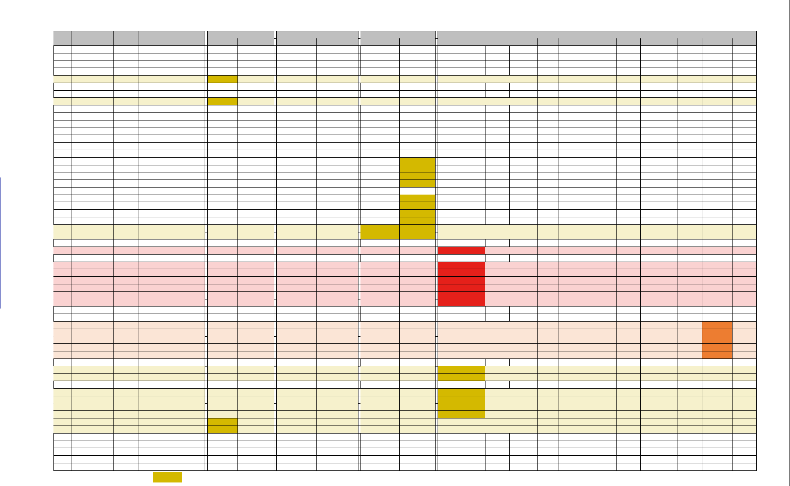
Appendix A – ESP32-S3 Consolidated Pin Overview
Appendix A – ESP32-S3 Consolidated Pin Overview
Pin Pin Pin Pin Providing Pin Settings RTC Function Analog Function IO MUX Function
No. Name Type Power At Reset After Reset 0 3 0 1 0 Type 1 Type 2 Type 3 Type 4 Type
1 LNA_IN Analog
2 VDD3P3 Power
3 VDD3P3 Power
4 CHIP_PU Analog VDD3P3_RTC
5 GPIO0 IO VDD3P3_RTC IE, WPU IE, WPU RTC_GPIO0 sar_i2c_scl_0 GPIO0 I/O/T GPIO0 I/O/T
6 GPIO1 IO VDD3P3_RTC IE IE RTC_GPIO1 sar_i2c_sda_0 TOUCH1 ADC1_CH0 GPIO1 I/O/T GPIO1 I/O/T
7 GPIO2 IO VDD3P3_RTC IE IE RTC_GPIO2 sar_i2c_scl_1 TOUCH2 ADC1_CH1 GPIO2 I/O/T GPIO2 I/O/T
8 GPIO3 IO VDD3P3_RTC IE IE RTC_GPIO3 sar_i2c_sda_1 TOUCH3 ADC1_CH2 GPIO3 I/O/T GPIO3 I/O/T
9 GPIO4 IO VDD3P3_RTC RTC_GPIO4 TOUCH4 ADC1_CH3 GPIO4 I/O/T GPIO4 I/O/T
10 GPIO5 IO VDD3P3_RTC RTC_GPIO5 TOUCH5 ADC1_CH4 GPIO5 I/O/T GPIO5 I/O/T
11 GPIO6 IO VDD3P3_RTC RTC_GPIO6 TOUCH6 ADC1_CH5 GPIO6 I/O/T GPIO6 I/O/T
12 GPIO7 IO VDD3P3_RTC RTC_GPIO7 TOUCH7 ADC1_CH6 GPIO7 I/O/T GPIO7 I/O/T
13 GPIO8 IO VDD3P3_RTC RTC_GPIO8 TOUCH8 ADC1_CH7 GPIO8 I/O/T GPIO8 I/O/T SUBSPICS1 O/T
14 GPIO9 IO VDD3P3_RTC IE RTC_GPIO9 TOUCH9 ADC1_CH8 GPIO9 I/O/T GPIO9 I/O/T SUBSPIHD I1/O/T FSPIHD I1/O/T
15 GPIO10 IO VDD3P3_RTC IE RTC_GPIO10 TOUCH10 ADC1_CH9 GPIO10 I/O/T GPIO10 I/O/T FSPIIO4 I1/O/T SUBSPICS0 O/T FSPICS0 I1/O/T
16 GPIO11 IO VDD3P3_RTC IE RTC_GPIO11 TOUCH11 ADC2_CH0 GPIO11 I/O/T GPIO11 I/O/T FSPIIO5 I1/O/T SUBSPID I1/O/T FSPID I1/O/T
17 GPIO12 IO VDD3P3_RTC IE RTC_GPIO12 TOUCH12 ADC2_CH1 GPIO12 I/O/T GPIO12 I/O/T FSPIIO6 I1/O/T SUBSPICLK O/T FSPICLK I1/O/T
18 GPIO13 IO VDD3P3_RTC IE RTC_GPIO13 TOUCH13 ADC2_CH2 GPIO13 I/O/T GPIO13 I/O/T FSPIIO7 I1/O/T SUBSPIQ I1/O/T FSPIQ I1/O/T
19 GPIO14 IO VDD3P3_RTC IE RTC_GPIO14 TOUCH14 ADC2_CH3 GPIO14 I/O/T GPIO14 I/O/T FSPIDQS O/T SUBSPIWP I1/O/T FSPIWP I1/O/T
20 VDD3P3_RTC Power
21 XTAL_32K_P IO VDD3P3_RTC RTC_GPIO15 XTAL_32K_P ADC2_CH4 GPIO15 I/O/T GPIO15 I/O/T U0RTS O
22 XTAL_32K_N IO VDD3P3_RTC RTC_GPIO16 XTAL_32K_N ADC2_CH5 GPIO16 I/O/T GPIO16 I/O/T U0CTS I1
23 GPIO17 IO VDD3P3_RTC IE RTC_GPIO17 ADC2_CH6 GPIO17 I/O/T GPIO17 I/O/T U1TXD O
24 GPIO18 IO VDD3P3_RTC IE RTC_GPIO18 ADC2_CH7 GPIO18 I/O/T GPIO18 I/O/T U1RXD I1 CLK_OUT3 O
25 GPIO19 IO VDD3P3_RTC RTC_GPIO19 USB_D- ADC2_CH8 GPIO19 I/O/T GPIO19 I/O/T U1RTS O CLK_OUT2 O
26 GPIO20 IO VDD3P3_RTC USB_PU USB_PU RTC_GPIO20 USB_D+ ADC2_CH9 GPIO20 I/O/T GPIO20 I/O/T U1CTS I1 CLK_OUT1 O
27 GPIO21 IO VDD3P3_RTC RTC_GPIO21 GPIO21 I/O/T GPIO21 I/O/T
28 SPICS1 IO VDD_SPI IE, WPU IE, WPU SPICS1 O/T GPIO26 I/O/T
29 VDD_SPI Power
30 SPIHD IO VDD_SPI IE, WPU IE, WPU SPIHD I1/O/T GPIO27 I/O/T
31 SPIWP IO VDD_SPI IE, WPU IE, WPU SPIWP I1/O/T GPIO28 I/O/T
32 SPICS0 IO VDD_SPI IE, WPU IE, WPU SPICS0 O/T GPIO29 I/O/T
33 SPICLK IO VDD_SPI IE, WPU IE, WPU SPICLK O/T GPIO30 I/O/T
34 SPIQ IO VDD_SPI IE, WPU IE, WPU SPIQ I1/O/T GPIO31 I/O/T
35 SPID IO VDD_SPI IE, WPU IE, WPU SPID I1/O/T GPIO32 I/O/T
36 SPICLK_N IO VDD_SPI / VDD3P3_CPU IE IE SPI CLK_N_DIFF O/T GPIO48 I/O/T SUBSPI CLK_N_DIFF O/T
37 SPICLK_P IO VDD_SPI / VDD3P3_CPU IE IE SPI CLK_P_DIFF O/T GPIO47 I/O/T SUBSPI CLK_P_DIFF O/T
38 GPIO33 IO VDD_SPI / VDD3P3_CPU IE GPIO33 I/O/T GPIO33 I/O/T FSPIHD I1/O/T SUBSPIHD I1/O/T SPIIO4 I1/O/T
39 GPIO34 IO VDD_SPI / VDD3P3_CPU IE GPIO34 I/O/T GPIO34 I/O/T FSPICS0 I1/O/T SUBSPICS0 O/T SPIIO5 I1/O/T
40 GPIO35 IO VDD_SPI / VDD3P3_CPU IE GPIO35 I/O/T GPIO35 I/O/T FSPID I1/O/T SUBSPID I1/O/T SPIIO6 I1/O/T
41 GPIO36 IO VDD_SPI / VDD3P3_CPU IE GPIO36 I/O/T GPIO36 I/O/T FSPICLK I1/O/T SUBSPICLK O/T SPIIO7 I1/O/T
42 GPIO37 IO VDD_SPI / VDD3P3_CPU IE GPIO37 I/O/T GPIO37 I/O/T FSPIQ I1/O/T SUBSPIQ I1/O/T SPIDQS I0/O/T
43 GPIO38 IO VDD3P3_CPU IE GPIO38 I/O/T GPIO38 I/O/T FSPIWP I1/O/T SUBSPIWP I1/O/T
44 MTCK IO VDD3P3_CPU IE* MTCK I1 GPIO39 I/O/T CLK_OUT3 O SUBSPICS1 O/T
45 MTDO IO VDD3P3_CPU IE MTDO O/T GPIO40 I/O/T CLK_OUT2 O
46 VDD3P3_CPU Power
47 MTDI IO VDD3P3_CPU IE MTDI I1 GPIO41 I/O/T CLK_OUT1 O
48 MTMS IO VDD3P3_CPU IE MTMS I1 GPIO42 I/O/T
49 U0TXD IO VDD3P3_CPU IE, WPU IE, WPU U0TXD O GPIO43 I/O/T CLK_OUT1 O
50 U0RXD IO VDD3P3_CPU IE, WPU IE, WPU U0RXD I1 GPIO44 I/O/T CLK_OUT2 O
51 GPIO45 IO VDD3P3_CPU IE, WPD IE, WPD GPIO45 I/O/T GPIO45 I/O/T
52 GPIO46 IO VDD3P3_CPU IE, WPD IE, WPD GPIO46 I/O/T GPIO46 I/O/T
53 XTAL_N Analog
54 XTAL_P Analog
55 VDDA Power
56 VDDA Power
57 GND Power
*
For details, see Section 2 Pins. Regarding highlighted cells, see Section 2.3.3 Restrictions for GPIOs and RTC_GPIOs.
Espressif Systems 71
Submit Documentation Feedback
ESP32-S3 Series Datasheet v1.8

Revision History
Revision History
Date Version Release notes
2023-11-24 v1.8
• Added chip variant ESP32-S3R16V and updated related information
• Added the second and third table notes in Table 1-1 Comparison
• Updated Section 2.6.1 Chip Boot Mode Control
• Updated Section 4.5 ADC Characteristics
• Other minor updates
2023-06 v1.7
• Removed the sample status for ESP32-S3FH4R2
• Updated Figure ESP32-S3 Functional Block Diagram and Figure 3-2 Com-
ponents and Power Domains
• Added the predefined settings at reset and after reset for GPIO20 in Table
2-1 Pin Overview
• Updated notes 5c, 5d, and 5e for Table 2-3 IO MUX and GPIO Pin Functions
• Updated the clock name “FOSC_CLK” to “RC_FAST_CLK” in Section 3.2.1
Power Management Unit (PMU)
• Updated descriptions in Section 3.5.2 Serial Peripheral Interface (SPI) and
Section 3.9.8 RSA Accelerator
• Other minor updates
2023-02 v1.6
• Improved the content in the following sections:
– Section Product Overview
– Section 2 Pins
– Section 3.2.1 Power Management Unit (PMU)
– Section 3.5.2 Serial Peripheral Interface (SPI)
– Section 4.1 Absolute Maximum Ratings
– Section 4.2 Recommended Power Supply Characteristics
– Section 4.3 VDD_SPI Output Characteristics
– Section 4.5 ADC Characteristics
• Added Appendix A
• Updated the notes in Section 1 ESP32-S3 Series Comparison and Section
5 Packaging
• Updated the effective measurement range in Table 4-5 ADC Characteristics
• Updated the Bluetooth maximum transmit power
• Other minor updates
Cont’d on next page
Espressif Systems 72
Submit Documentation Feedback
ESP32-S3 Series Datasheet v1.8

Revision History
Cont’d from previous page
Date Version Release notes
2022-12 v1.5
• Removed the ”External PA is supported” feature from Section Features
• Updated the ambient temperature for ESP32-S3FH4R2 from 40 ∼ 105
°C to 40 ∼ 85 °C
• Added two notes in Section 5
2022-11 v1.4
• Added the package information for ESP32-S3FH4R2 in Section 5
• Added ESP32-S3 Series SoC Errata in Section Related Documentation and
Resources
• Other minor updates
2022-09 v1.3
• Added a note about the maximum ambient temperature of R8 series chips
to Table 1-1 and Table 4-2
• Added information about power-up glitches for some pins in Section 2.2
• Added the information about VDD3P3 power pins to Table 2.2 and Section
2.5.2
• Updated section 3.7.1
• Added the fourth note in Table 2-1
• Updated the minimum and maximum values of Bluetooth LE RF transmit
power in Section 4.9.1
• Other minor updates
2022-07 v1.2
• Updated description of ROM code printing in Section 2.6
• Updated Figure ESP32-S3 Functional Block Diagram
• Update Section 4.6
• Deleted the hyperlinks in Application
2022-04 v1.1
• Synchronized eFuse size throughout
• Updated pin description in Table 2-1
• Updated SPI resistance in Table 4-3
• Added information about chip ESP32-S3FH4R2
Cont’d on next page
Espressif Systems 73
Submit Documentation Feedback
ESP32-S3 Series Datasheet v1.8

Revision History
Cont’d from previous page
Date Version Release notes
2022-01 v1.0
• Added wake-up sources for Deep-sleep mode
• Added Table 2-12 for default configurations of VDD_SPI
• Added ADC calibration results in Table 4-5
• Added typical values when all peripherals and peripheral clocks are enabled
to Table 4-8
• Added more descriptions of modules/peripherals in Section 3
• Updated Figure ESP32-S3 Functional Block Diagram
• Updated JEDEC specification
• Updated Wi-Fi RF data in Section 4.6
• Updated temperature for ESP32-S3R8 and ESP32-S3R8V
• Updated description of Deep-sleep mode in Table 4-9
• Updated wording throughout
2021-10-12 v0.6.1 Updated text description
2021-09-30 v0.6
• Updated to chip revision 1 by swapping pin 53 and pin 54 (XTAL_P and
XTAL_N)
• Updated Figure ESP32-S3 Functional Block Diagram
• Added CoreMark score in section Features
• Updated Section 2.6
• Added data for cumulative IO output current in Table 4-1
• Added data for Modem-sleep current consumption in Table 4-8
• Updated data in section 4.6, 4.8, and 4.9
• Updated wording throughout
2021-07-19 v0.5.1
• Added ”for chip revision 0” on cover, in footer and watermark to indicate
that the current and previous versions of this datasheet are for chip version
0
• Corrected a few typos
2021-07-09 v0.5 Preliminary version
Espressif Systems 74
Submit Documentation Feedback
ESP32-S3 Series Datasheet v1.8

www.espressif.com
Disclaimer and Copyright Notice
Information in this document, including URL references, is subject to change without notice.
ALL THIRD PARTY S INFORMATION IN THIS DOCUMENT IS PROVIDED AS IS WITH NO
WARRANTIES TO ITS AUTHENTICITY AND ACCURACY.
NO WARRANTY IS PROVIDED TO THIS DOCUMENT FOR ITS MERCHANTABILITY, NON-
INFRINGEMENT, FITNESS FOR ANY PARTICULAR PURPOSE, NOR DOES ANY WARRANTY
OTHERWISE ARISING OUT OF ANY PROPOSAL, SPECIFICATION OR SAMPLE.
All liability, including liability for infringement of any proprietary rights, relating to use of information
in this document is disclaimed. No licenses express or implied, by estoppel or otherwise, to any
intellectual property rights are granted herein.
The Wi-Fi Alliance Member logo is a trademark of the Wi-Fi Alliance. The Bluetooth logo is a
registered trademark of Bluetooth SIG.
All trade names, trademarks and registered trademarks mentioned in this document are property
of their respective owners, and are hereby acknowledged.
Copyright © 2023 Espressif Systems (Shanghai) Co., Ltd. All rights reserved.
